| Quantity | Price(USD) | Ship Date |
|---|---|---|
| 1-10 | TBD | |
| 10- | TBD |
NOTE : Ship Dates above are subject to change depending upon availability.

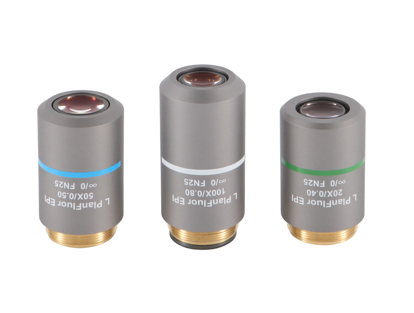
It maintains a long working distance even at high magnification (3.1mm, far exceeding that of conventional 100× objectives), balancing high resolution with operational safety; a numerical aperture (NA) of 0.8 enhances light-gathering capability, and combined with a flat-field semi-apochromatic design, it achieves high-definition, color-fringe-free imaging across the entire field of view.
Applications include:
Ultra-fine inspection of semiconductor nano-defects (such as pinholes in wafer oxide layers), micro-morphologies of ultra-precision materials (such as graphene), etc.
| NA | 0.8 | WD | 3.1mm |
| R | 0.34um | ±D.F | 0.43um |
| Quantity | Price(USD) | Ship Date |
|---|---|---|
| 1-10 | TBD | |
| 10- | TBD |