Near-infrared enhanced silicon PIN photodiode (COB package)

https://source.venuslabtech.com/mall-prod/76e5a5ae-88a9-4efd-bf2b-e9c10802d59b.png

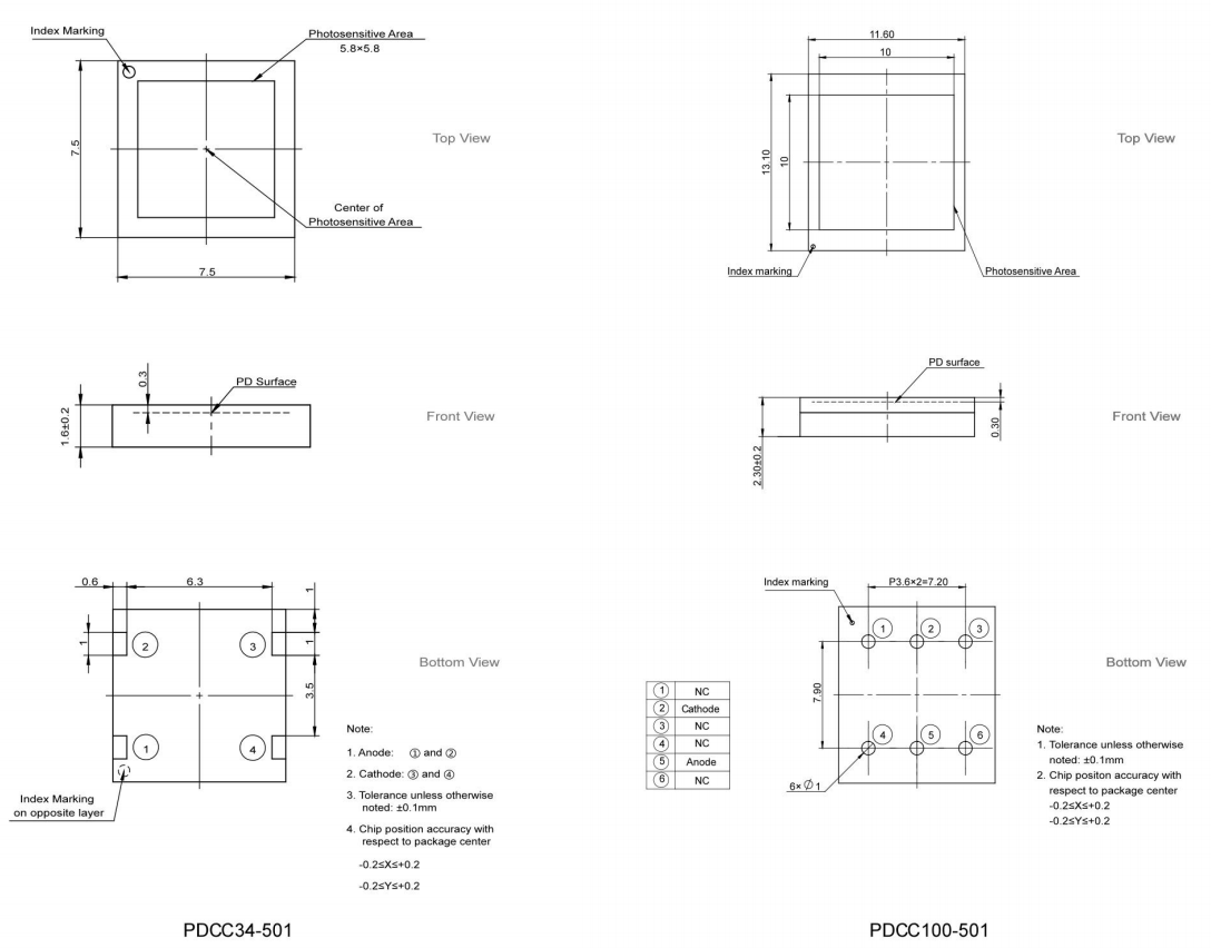
Silicon-based PIN structure photoelectric conversion devices optimized for response efficiency in the near-infrared band

  • Enhanced near-infrared response
    • Low dark current and high precision
    • Resistance to basic environments
    • Friendly to mass production costs
Enter your email address to get free access, receive a product brochure, or enjoy special discounts.
Overview
Specifications
Applications

Introduction:

This device has a spectral response range covering 350~1100nm, featuring both optimized near-infrared wavelength response and low dark current characteristics. It is suitable for photoelectric measurement instruments, optical analysis equipment, and optical power monitoring scenarios.


It accurately converts near-infrared light signals into electrical signals, especially overcoming the shortcoming of ordinary silicon PIN photodiodes in their response to the near-infrared band, making them suitable for scenarios such as near-infrared detection, communication, and sensing.


Features:

  • Wire bonding with low resistance and low loss
    • Near-infrared custom anti-reflection coating to prevent stray light
    • Multi-chip array with precise spacing control
    • Package protective layer selected according to needs
    • Low junction capacitance, suitable for high-frequency signals
    • Low temperature drift to ensure data consistency


Dimension:

Explore Series

Near-Infrared Enhanced Silicon PIN Photodiode (COB Package)

PDCC34-501
Photosensitive surface size 5.8×5.8mm.
Ships as soon as Same Day
Stock Items Included

Near-infrared enhanced silicon PIN photodiode (COB package)

PDCC100-501
The size of the photosensitive surface is 10×10mm.
Ships as soon as Same Day
Stock Items Included
Telegram LogoWhatsApp Logo