Join Venus Lab Inner Lens for exclusive
science and product updates.
When you sign up for our insider updates, we’ll handle your
personal information with care and in accordance with our
privacy policy.
Professional-grade microscopic imaging and industrial inspection scenarios
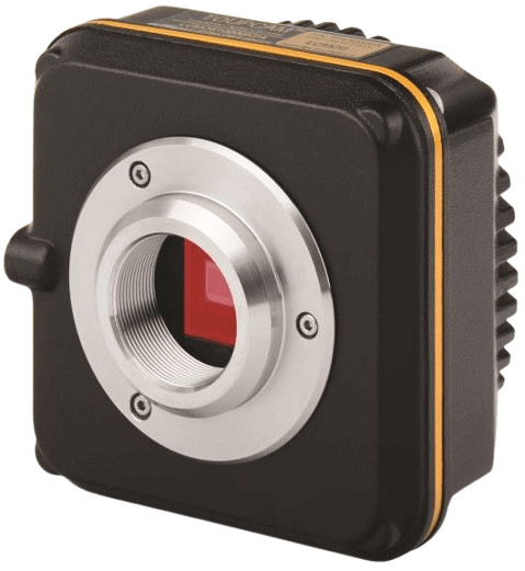
The Venuslab-L3 CMOS Camera is a high-end professional imaging device launched by Venuslab. It features a core architecture of "Aptina high-performance CMOS sensor + on-board cache + USB3.0 high-speed transmission". Its resolution ranges from 1.2M to 14M pixels, catering to different precision requirements. The camera adopts a standard C-mount design, which is compatible with mainstream brand microscopes such as NIKON and LEICA. It has a built-in Ultra-Fine color engine and a high-quality IR-CUT filter, enabling accurate color reproduction in the 380-650nm spectral range. Coupled with a natural heat dissipation structure, it effectively reduces image noise. Relying on the USB3.0 5Gbps high-speed interface and multi-level pixel binning technology, the 14M pixel model can achieve a frame rate of 53.3fps in 4×4 binning mode, while the on-board cache ensures the stability of data transmission. The software comes standard with the ToupView image processing application, offering SDKs for multiple platforms such as Windows and Linux, as well as rich programming interfaces, which are suitable for secondary development needs. It is widely used in scenarios such as brightfield microscopic imaging, industrial inspection, scientific research and education, and can operate stably in a wide temperature range of -10℃ to 50℃.
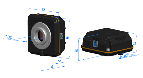
Schematic diagram of the external dimensions of the Venuslab-L3 CMOS Camera. The camera housing is made of hard aluminum alloy through machining, ensuring resistance to impact under heavy load conditions. A high-quality IR-CUT is installed at the front end of the camera sensor, which mainly functions to filter out infrared light waves in imaging and protect the camera sensor at the same time. Compared with cameras of other brands, Venuslab's cameras have no moving parts to ensure that the camera is sturdy, reliable, and durable. At the same time, there is no image blurring caused by the shaking of moving parts.