Automated Optical Inspection: A Vision Workflow for High-Density PCB Defect Detection
Author: D. Miller, Lead Vision Systems Integrator
In modern electronics manufacturing, component density is skyrocketing. With 01005 micro-components and complex Ball Grid Arrays (BGAs), manual visual inspection is completely obsolete. To guarantee zero-defect assemblies at line speed, we developed a custom inline Automated Optical Inspection (AOI) and Solder Paste Inspection (SPI) station. Here is the hardware architecture we rely on to catch missing parts, tombstones, and solder bridges in milliseconds.
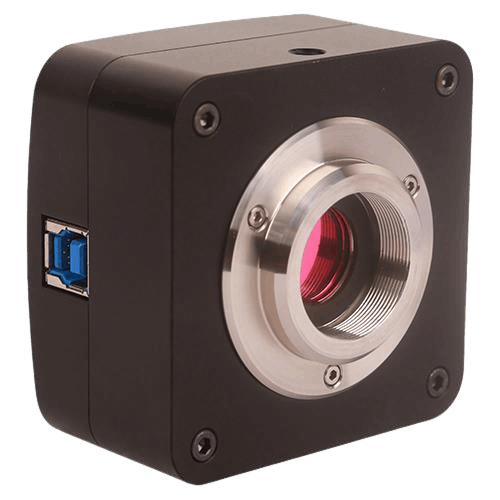
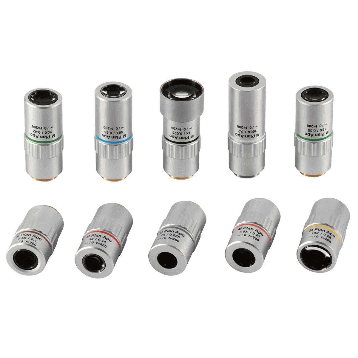
1. High-Fidelity Image Acquisition
Capturing a fast-moving PCB without motion blur requires high-speed, global shutter technology. We integrated industrial-grade CMOS Cameras paired with low-distortion telecentric Imaging Optics. The high megapixel count allows us to maintain a large field of view (FOV) to inspect multiple components simultaneously, while still resolving the microscopic details of fine-pitch IC pins.
2. Conquering Reflective Surfaces with Dynamic Lighting
Solder joints act like tiny, curved mirrors. Traditional coaxial lighting causes intense glare, masking true defects. Our solution relies on programmable, multi-angle dome and ring lighting powered by high-intensity LED. By flashing different lighting angles in rapid sequence (RGB/W), we can extract topological data based on color gradients and clearly define the exact shape and angle of every solder meniscus.
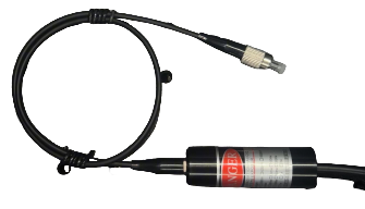
3. 3D Structural Profiling for Volume Measurement
While 2D imaging easily finds missing or misaligned components, it cannot accurately measure the volume of solder paste—a critical metric for preventing weak joints. We project precision structured light patterns across the board using industrial Laser Modules. The camera reads the deformation of these laser lines over the components, allowing our software to construct a full 3D height map of the PCB surface.
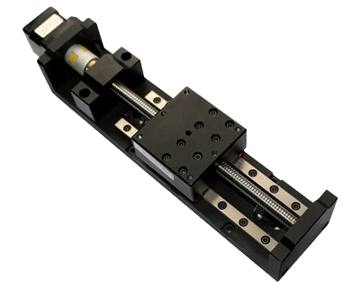
4. Precision High-Speed Indexing
To match the rapid beat rate of our Surface Mount Technology (SMT) line, the imaging system must step across large, multi-board panels in seconds. We mounted our heavy optical payload on high-velocity Motorized Stages. These stages provide the rigid, vibration-free rapid acceleration and deceleration necessary to perform high-speed scanning without losing micrometer-level positional accuracy.
Conclusion
By combining global shutter imaging, multi-angle LED illumination, laser-based 3D profiling, and high-speed motion control, we deployed an AOI system that keeps pace with our fastest SMT lines. This workflow drastically reduced our false call rates and ensured that only perfectly assembled boards move on to final testing.