| 数量 | 价格(USD) | 发货日期 |
|---|---|---|
| 1-10 | 待定 | |
| 10- | 待定 |
注意:发货日期以上是因库存不足而调整的。
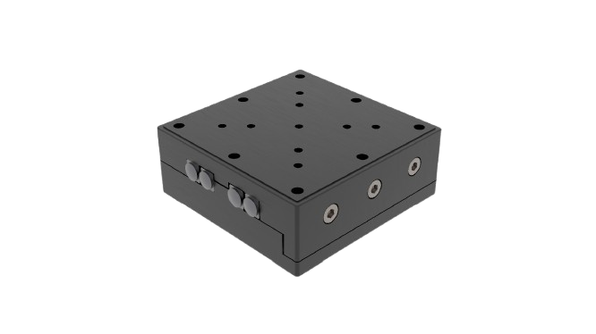
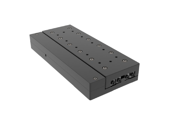
Advantages: Large field of view + nano-precision; piezo direct drive eliminates lead screw backlash for cross-scale precision scanning.
Differentiation: Rare compact solution balancing 8-inch wafer range and submicron positioning.
Applications: Semiconductor wafer defect inspection, full-scan of large biological sections, panel testing.
| Travel Range | Resolution | Max Load |
|---|---|---|
| 250 × 250 mm | 50 nm | 10.0 kg |
| 数量 | 价格(USD) | 发货日期 |
|---|---|---|
| 1-10 | 待定 | |
| 10- | 待定 |