| Quantity | Price(USD) | Ship Date |
|---|---|---|
| 1-10 | TBD | |
| 10- | TBD |
NOTE : Ship Dates above are subject to change depending upon availability.

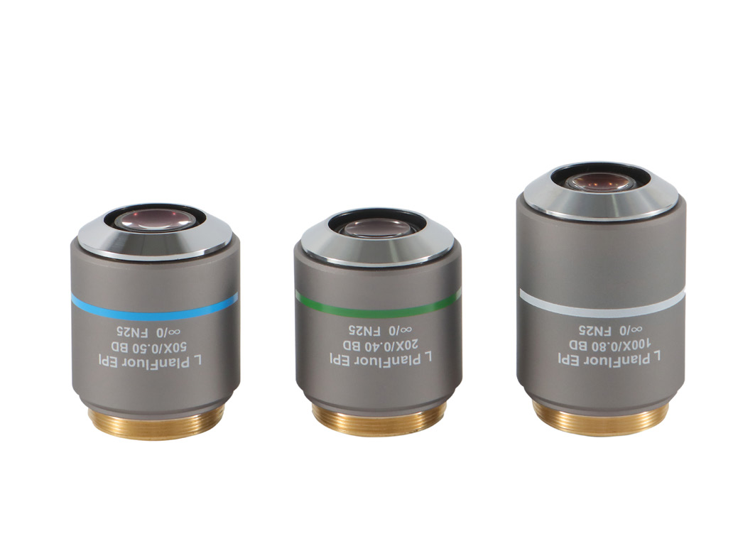
Breakthrough in long working distance at high magnification: With a working distance of 3.1mm, it far exceeds that of conventional 100× objectives (usually < 1mm), balancing ultra-precise observation and operational safety; Ultimate resolution: NA 0.8 combined with flat-field semi-apochromatism enables detection of ultra-fine defects such as nanoscale short circuits in chips and pinholes in wafer oxide layers.
Applications include:
Nanoscale scratch detection of semiconductor chips (dark field), microtopography analysis of ultra-precision materials (such as graphene) (bright field), and high-magnification observation of abnormal metal grain boundaries.
| NA | 0.8 | WD | 3.1mm |
| R | 0.34um | ±D.F | 0.43um |
| Quantity | Price(USD) | Ship Date |
|---|---|---|
| 1-10 | TBD | |
| 10- | TBD |