Join Venus Lab Inner Lens for exclusive
science and product updates.
When you sign up for our insider updates, we’ll handle your
personal information with care and in accordance with our
privacy policy.
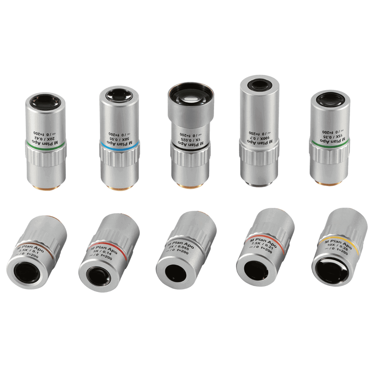
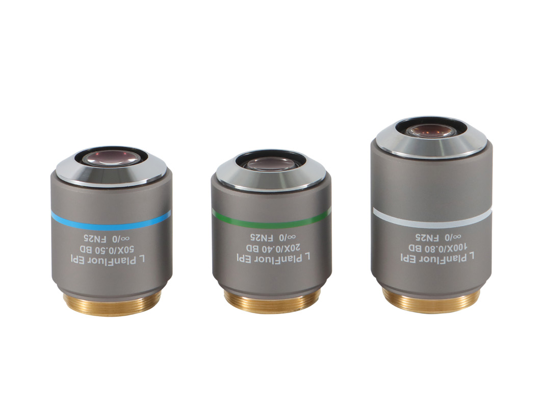
The objective lens of VenusLab microscope is the core imaging component of an optical microscope. It is responsible for collecting the reflected/transmitted light from microscopic samples and converging it to form an image. Working in synergy with the microscope camera, it enables "high-magnification and high-definition microscopic observation".Different from other optical components, it directly determines the imaging resolution and clarity, and serves as a key element in microscopic analysis for biology, materials science, and industrial applications.
The core optical component for professional-grade brightfield imaging

Ultra - wide field of view + extremely large depth of focus. It maintains a 13mm working distance at low magnification and allows for a certain degree of undulation on the sample surface (the 440μm depth of focus covers a wide range of height differences).
It can be applied to the full - panel scanning of PCB boards/wafers, the surface defect screening of large - sized parts, and automated production lines that need to integrate laser processing heads (the large spacing avoids collisions).
A benchmark for ultra-long working distance: the 34mm spacing enables observation of ultra-thick/irregular samples (e.g., 3D printed parts, transparent thick films), while achieving a 5μm resolution (twice that of the 1X model).
It can be applied to thickness inspection of new energy battery pole pieces (thick coatings) and non-destructive observation of samples with complex morphologies (e.g., surfaces of cast and forged parts).

Ultra-long working distance of 41mm, which can almost accommodate finger operations, suitable for large samples or scenarios requiring tool intervention; Medium and low magnification transition: 2.8μm resolution, significantly improved compared to 1X/2X, balancing field of view and details.
Applied to :
electronic component inspection (such as PCB boards), mineral particle observation, and local fine analysis of large-volume samples.

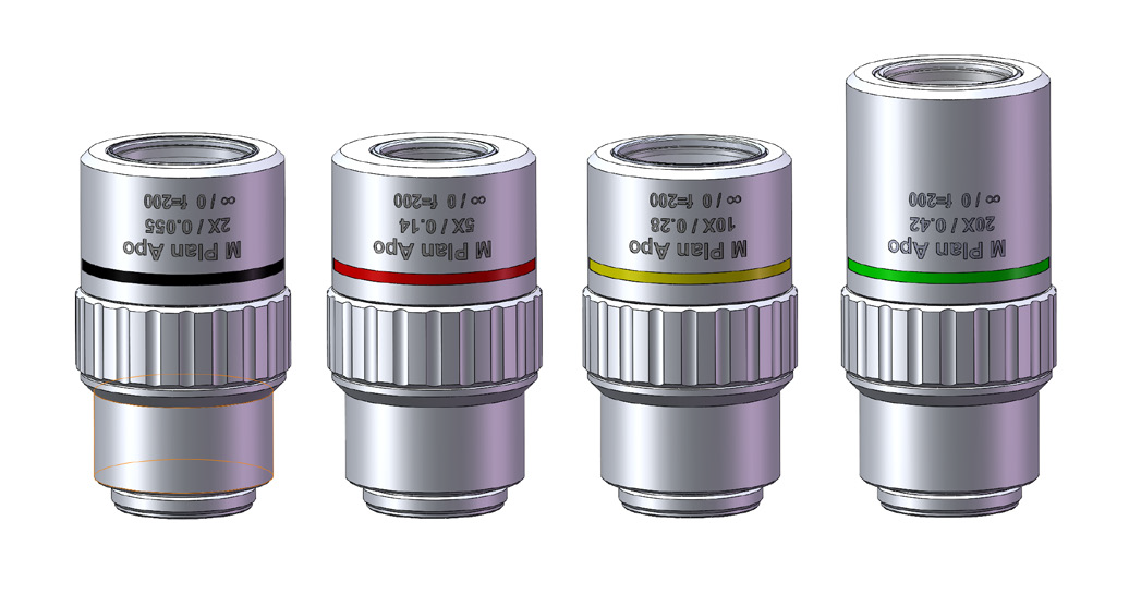
Low-to-medium magnification "balancer": NA=0.14 improves resolution (2.0μm), with a 35mm working distance still retaining operational space; a cost-effective choice: balancing magnification, resolution and practicality, suitable for low-to-medium magnification observation in conventional laboratories.
It can be applied to cell colony observation, fiber diameter measurement, and preliminary analysis of metal grains.

The "performance inflection point" of medium-magnification observation, through the breakthrough in numerical aperture (NA), chromatic aberration correction, and the maintenance of effective working distance, organically integrates "field of view breadth" and "detail depth".
It precisely adapts to niche scenarios such as cell morphology observation, material defect detection, and biological structure analysis, thus becoming an efficient choice for medium-magnification observation in laboratories.

Classic "Universal Lens": 10x magnification + NA=0.28, balancing resolution (1.0μm) and working distance (34mm), suitable for over 90% of conventional observations; lightweight and efficient: 217g weight is friendly to microscope loads, making long-term observation less tiring.
It is applied to the observation of intracellular structures (such as cell nuclei), bacterial morphology, and grain structures on metal polished surfaces.

Medium-high magnification "transition bridge": NA = 0.35 improves resolution (0.8μm), and the 22mm working distance still supports limited operations (such as fine-tuning samples); Detailed deepening: 20% higher resolution than 10X, suitable for observing organelles and fiber details.
Applied to :
mitochondrial observation, fiber woven structures, and semiconductor chip circuit line analysis.

High-power "precision eye": NA=0.42, close to the lower limit of oil immersion lenses, with a resolution of 0.7μm, reaching submicron depth; Narrow depth of focus: ±1.6μm, requiring flatter samples, suitable for ultra-thin sections or fine focusing.
Applied to the observation of organelle details (such as the Golgi apparatus), virus particles (after staining), and metal phase boundaries.

High-magnification "core lens": NA=0.55 enables a resolution of 0.5μm under 50x magnification (close to the diffraction limit of 550nm wavelength); extremely narrow field of view: a 0.48mm field of view requires precise positioning, suitable for observing single cells and nanostructures.
Applied in the analysis of nuclear substructures, nanoparticles, and metal twin boundaries.

NA = 0.7 + 100x magnification, achieving a resolution of 0.4μm (theoretical maximum at 550nm), approaching the limit of optical microscopes; a working distance of 6mm requires strict light control (it is recommended to use a coverslip), and the extremely shallow depth of focus (±0.56μm) has extremely high requirements for the flatness of the sample.
It is applied to the observation of virus morphology (high staining degree), protein crystals, and semiconductor quantum dots.
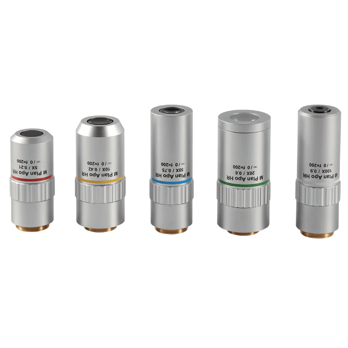
High-order brightfield imaging + quantitative analysis

A 25mm WD still falls into the “long - working - distance” category (longer than the high - magnification HR models in the same series).
However, the NA jumps to 0.21, and the resolution breaks through to 1.3μm (close to the performance of medium - magnification lenses), balancing the operational space and detailed observation.

After the numerical aperture (NA) exceeds 0.42, the resolution reaches the sub-micron level (0.7μm). With a 15mm working distance (WD),
it still supports limited operations (e.g., auxiliary micro-operation), making it a universal high-resolution model for industrial quality inspection and scientific research.

NA=0.6 balances resolving power (0.5μm) and working distance (9.5mm), allowing observation of submicron structures without oil immersion; the value of flat-field design is prominent: the entire field of view is clear at 20x magnification, compatible with 1" cameras (0.48×0.64mm field of view) for capturing distortion-free images.
Applications:
Fine structures of organelles (such as mitochondrial cristae, Golgi apparatus);
Measurement of semiconductor circuit line width (≤1μm line width);
Detection of interlayer defects in thin films (such as delamination of photovoltaic films).
Dry lens "peak performance": NA=0.75 + 50x magnification, 0.4μm resolution approaching the 550nm wavelength diffraction limit (theoretical ~0.41μm); 5.2mm working distance breakthrough: still retaining an operating space of more than 5mm under high NA, suitable for ultra-thin sections (≤5μm) or chip observation.
Applications:

NA = 0.9 + 100x magnification, with a resolution of 0.3μm that exceeds the recognition limit of the human eye (image assistance required); a working distance of 1.4mm requires ultra-thin and flat samples (≤1μm) + cover glass, and apochromatism ensures accurate colors under high magnification.
Applications:
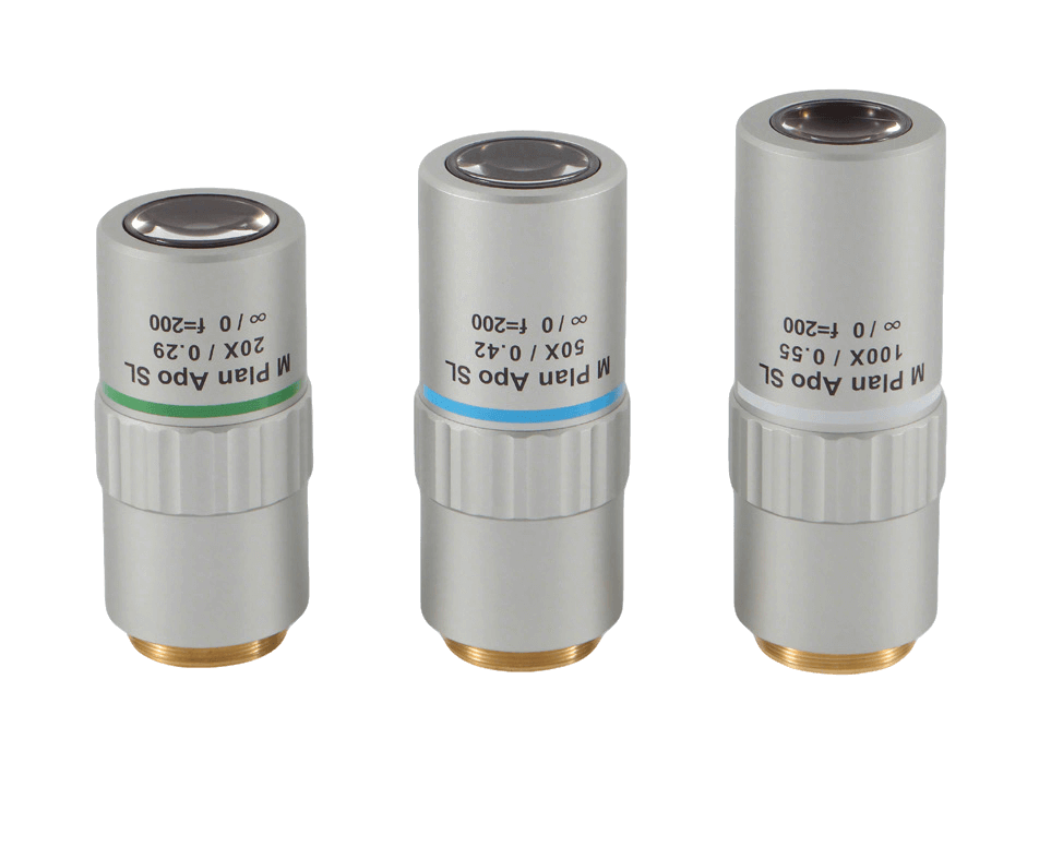
VL Plan Apo SL is the "high-end configuration" in brightfield observation, widely used in industrial inspection, materials science, and quality control.
20× "Micromanipulation Companion": A 30mm working distance provides ample space for tweezers gripping and liquid dropping, adapting to layered observation of thick samples (such as 10-15μm plant sections), eliminating the limitation of "high magnification requiring sample attachment"; Apochromatic correction ensures stable basic image quality: during brightfield observation, there is no color shift at cell boundaries and stained areas, meeting the needs of routine pathological section examination and initial screening of material defects.
Applications:
Analysis of multi-layer structures in plant vascular bundles, auxiliary observation of cell cluster microinjection, general inspection of surface defects in PCB circuits.

50× Class "Balance King": NA increased to 0.42, resolution jumped to 0.7μm (clearly distinguishable mitochondrial cristae), 20mm working distance still supports fine adjustment of the stage, breaking the contradiction of "high resolution must lose operability"; Apochromatic anti-distortion: the edge and center in the 1" camera field of view (0.19×0.26mm) have the same clarity, suitable for quantitative analysis of metal grain boundaries and thin film pinhole defects.
Applied to:
Observation of cell organelle details, analysis of aluminum alloy aging phases, positioning of defects between photovoltaic film layers

100× "User-Friendly Extreme Lens": A 13mm working distance allows fine focusing on ultra-thin samples (≤5μm), avoiding the "blur on contact" issue of conventional high-power lenses; NA=0.55 + apochromatic correction, achieving both excellent color and clarity at high magnification, breaking through the bottleneck in observing submicron structures (such as viral morphology, nanoparticles);
Applications:
Analysis of stained viral envelope structures, measurement of semiconductor gate linewidths (≤0.5μm), ultra-fine observation of kaolinite lamellae.
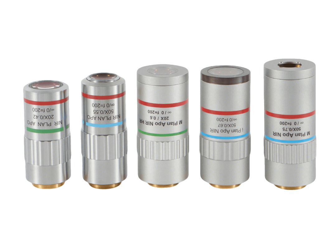
Synergistic Innovation in Photopic and Near-Infrared Processing, widely used in scientific research, industrial inspection, and equipment integration.

20mm long-distance adaptation for near-infrared transillumination of thick samples (such as silicon wafers, plant stems) with sufficient operating space; apochromatic correction for chromatic aberration in the 800-1200nm range, ensuring no color shift in near-infrared fluorescent labeling (such as Cy5.5) imaging, clearly presenting the contours of deep cells.
Applications:
Near-infrared deep imaging of living cells, internal defect inspection of silicon wafers, transillumination analysis of plant vascular bundles.

NA is increased to 0.55, breaking through the 0.5μm resolution, capable of distinguishing quantum dots and semiconductor defects; the 13mm working distance supports fine adjustment of the stage, adapting to near-infrared microscopy for glass impurities and interlayer defects in thin films.
Applied to:
Near-infrared fluorescent organelle observation, photovoltaic film defect localization, and nanoparticle size analysis.

NA=0.6+HR design, breaking through the near-infrared diffraction limit, capable of resolving submicron circuits on silicon wafers and deep biological blood vessels; a 9.5mm working distance balances high resolution and operability, suitable for failure analysis of semiconductor chips (such as gold wire bonding defects).
Applied to:
High-resolution detection of semiconductor circuits, NIR imaging of cerebral cortical blood vessels, and quantum well luminescence analysis.
Flat field design + NA=0.67, the edge and center of the full field of view are equally clear, suitable for imaging with near-infrared detector chips and quantum dot arrays; a 10mm working distance supports fine focusing, making it suitable for near-infrared super-resolution observation of ultra-thin samples (≤5μm).
Applications:
Near-infrared detector pixel analysis, quantum dot luminescence pattern detection, quantitative analysis of single-cell fluorescence signals.

NA = 0.75 + HR design, with a resolution of 0.37μm breaking through the near-infrared limit, presenting semiconductor nanostructures and near-infrared labeling of viruses; a short distance of 4mm is used to achieve high NA, suitable for ultra-fine observation of ultra-thin window sheets and quantum device chips.
Applications include:
Graphene wrinkle analysis, virus NIR morphology observation, and semiconductor nanowire array detection.
It is a high-end near-infrared objective exclusively for the liquid crystal industry.
• Optical correction: flat field + apochromatic, achieving "full-field precise imaging"
• Near-infrared exclusive: penetrating glass + compatible with laser processing
• Customized glass compensation: adapting to liquid crystal substrates of different thicknesses
• Long working distance + infinite correction: safer and more flexible operation
• Bright field optimization: sharp contrast, details "distinguishable at a glance"

T0 compensation with 0mm glass, suitable for ultra-thin / substrate-free samples. The flat-field design ensures that the edge and center of the field of view are clear simultaneously, with no color fringing interference in the near-infrared band.
Applications:
Liquid crystal research and development (thin sample testing), defect detection of transparent films, or observation of large spacing of protrusions on the sample surface.

Custom correction of aberrations for 0.7mm glass, with high near-infrared penetration to "see through" the substrate and restore details of internal circuits.
Application:
Routine inspection of LCD production lines (mobile phone / display panels), for rapid screening of line breaks and pixel defects.

It counteracts the aberration diffusion of thick glass. The flat-field design ensures clear edges in a large field of view, balancing efficiency and precision.
Applications:
Inspection of large-sized liquid crystal panels (TVs / industrial control screens), or large-field-of-view observation of multi-layer glass devices.

t0 compensation with 0mm glass, high NA + apochromatism achieve fine near-infrared imaging, and flat-field design eliminates high-magnification edge blurring.
Applications:
Detection of tiny liquid crystal defects (micron-level scratches/bubbles), observation of OLED microcircuits, or scientific research-level near-infrared analysis.

Targeted correction of 0.7mm glass aberration at high magnification, restoring pixel-level details under the substrate, compatible with coaxial observation of near-infrared laser processing.
Applications:
High-end liquid crystal quality inspection (such as in Apple's supply chain), pixel defect analysis, or real-time monitoring of laser repair.
Break through the aberration bottleneck of "thick sample + high magnification", and clearly present the deep structure of thick substrates (such as multi-layer circuit intersection areas) in the near-infrared range.
Applications:
Depth defect analysis of large-sized thick glass panels (automotive/medical screens), and microscopic research on liquid crystal materials.
A high-end optical device designed for the manufacturing and repair of liquid crystal panels.

Field flattening design eliminates field curvature, and a 20mm long working distance avoids collisions with protrusions; achromatic correction covers ultraviolet (355nm) + visible light, resulting in imaging without color fringing.
Applications:
Liquid crystal research and development stage: ultra-thin sample testing (such as experimental glassless substrates); surface defect detection of transparent films (such as OCA glue), or observation of semiconductor wafer dies (extended scenarios).

Custom correction for 0.7mm glass refraction interference, high transmittance in the near-ultraviolet (355nm) range + visible bright field, and simultaneous support for coaxial observation in laser processing (such as mobile phone screen pixel repair).
Applications:
Routine inspection in mobile phone/tablet LCD production lines (detection of circuit breaks, pixel defect screening);
Real-time monitoring of the processing area during 355nm laser repair (coaxial optical path, position error < 2μm).
It counteracts the aberration diffusion of thick glass, and the flat-field design ensures clear edges in a large field of view (such as the detection of an entire TV screen), balancing efficiency and accuracy.
Applications:
Full-field defect scanning of large-size liquid crystal panels (such as 8K TV screens);
Internal structure observation of multi-layer thick glass devices (such as in-vehicle display modules) (near-ultraviolet penetration + bright field contrast).

High NA + apochromatic correction enables fine ultraviolet-visible imaging, and flat-field design eliminates high-magnification edge blurring, making it suitable for research-grade analysis.
Applications include:
Liquid crystal micron-level defect analysis (such as 0.5μm scratches, bubbles);
Near-ultraviolet photoresist observation of semiconductor wafers (optimized for 355nm wavelength, compatible with lithography processes).

Targeted correction of 0.7mm glass aberration at high magnification, restoring pixel-level details of mobile phone screens, and supporting 355nm laser repair coaxial monitoring (such as OLED pixel electrode repair).
Applications:
High-end liquid crystal quality inspection (such as Apple's supply chain) for quantitative analysis of pixel defects;
Real-time monitoring of laser repair (such as ITO circuit repair, with a spot accuracy of 0.1μm).

Break through the aberration bottleneck of "thick glass + high magnification", clearly present the deep structure of thick substrates (such as multi-layer circuit crossing areas) in the near-ultraviolet range, and be compatible with laser processing.
Applications include:
Depth defect analysis of large-sized thick glass panels (automotive/medical screens) (such as circuit short circuits under 1.1mm glass);
Near-ultraviolet spectral research on liquid crystal materials (apochromatism ensures the accuracy of multi-wavelength data).
Infinity-Corrected Brightfield Flat-Field Apochromatic Objectives
• Full-band apochromatic correction: precise focusing from near-ultraviolet to visible light
• High numerical aperture of the HR version breaks through the resolution limit
• Design with long working distance and compatibility with laser processing
• Flat-field apochromatic design ensures clarity across the entire field of view
• Infinity correction and flexibility in system integration
• Environmentally friendly materials and adaptation to special scenarios
Ultra-long and wide field of view: 2× low magnification + 30.5mm ultra-long working distance. When matched with a Φ24 eyepiece, the actual field of view reaches 12mm, which can cover large-sized samples at one time (such as the edge of an entire wafer), reducing stitching observation errors. Apochromatic adaptation: Synchronous correction for 355nm ultraviolet and 532nm visible light, suitable for rapid dual-band scanning (ultraviolet-visible) of large-scale samples (such as initial positioning of semiconductor wafers, global inspection of LCD panels).
Applications:
"Rapid screening" of large-sized samples in industrial production lines, or area positioning before laser processing.

"Long-distance + medium magnification" balance: The combination of a 30.5mm working distance and 5× magnification not only retains a large operating space (suitable for fixtures and light sources) but also improves the resolution to 2.1μm, enabling observation of medium-level details (such as LCD pixel arrays and chip packaging contours). Multi-band compatibility: Achromatic aberration correction in the 355-532nm range, supporting simultaneous ultraviolet laser processing and visible light observation (e.g., real-time monitoring of laser cutting areas).
Applications:
Defect detection in electronic component packaging, "regional-level" detail observation in laser micromachining.

"Ultra-long distance + high resolution" breakthrough: maintaining a working distance of 30.5mm at 10× magnification (far exceeding the 10-15mm of conventional 10× objectives), while the NA is increased to 0.28 and the resolution reaches 1μm, meeting the dual requirements of "long operating space + precise observation". Parfocal advantage: a 95mm conjugate distance ensures that the focus remains unchanged when switching with 2×/5× objectives, improving the efficiency of multi-magnification observation.
Applications:
Inspection of samples with complex fixtures (such as flip chips), observation of laser etching requiring manual operation space.

The 20X model with a 17mm working distance, which is better than the conventional 20× (generally < 10mm), is suitable for observing medium details such as chip pins and circuit line widths, balancing magnification and operating space. The 355nm ultraviolet light captures details of photoresist, and the 532nm visible light restores the color of metal circuits, supporting dual-band quality inspection for semiconductor lithography/etching.
Applications:
Semiconductor circuit line width measurement (≥0.7μm), LCD color filter defect detection.

HR version NA 0.8, optimized for 355nm, with a resolution of 0.3μm (near the diffraction limit), capable of distinguishing submicron structures such as chip nanocircuits. The short working distance of 1.6mm is a compromise for high NA, suitable for ultra-fine observation of fixed samples such as semiconductor wafer defect re-judgment and laser processing endpoint detection.
Applied in:
Detection of advanced semiconductor processes (such as circuits below 7nm), verification of "endpoint accuracy" in laser micro-nano processing.
Widely used in metallographic defect detection, semiconductor chip observation, and material microscopic analysis
Low magnification with a large field of view + ultra-long working distance, flat-field apochromatism ensures clear edges of the 20mm field of view; achromatism across the entire 400-700nm wavelength range, with no "color fringing" in colors.
Applications:
Macro scanning of large-sized samples (such as preliminary screening of surface defects on metal plates, global positioning of wafers). The long working distance allows direct observation of bulk samples up to 20mm thick without removing accessories.

Medium magnification balances range and detail. The NA improvement enables a resolution of 2μm (2.5 times higher than that of 2×), and the flat-field design ensures consistent clarity between the edge and center of the field of view.
Applications include:
Observation of metal grain distribution and semiconductor packaging textures. The long working distance is suitable for samples with convex structures (such as welded parts and chip pins). A polarizing module can be added to analyze crystal orientation.

High magnification, full field of view with uniform clarity. NA=0.28 achieves 1μm-level resolution. Flat-field correction eliminates "edge blurring"; the infinite conjugate architecture is compatible with high-pixel cameras (2.3×3.07mm field of view).
Applications:
Routine high-magnification analysis. The long working distance allows the addition of a DIC prism, expanding differential interference observation.
Nanoscale detail reproduction, NA=0.42 + apochromatism, achieving 0.7μm resolution (close to the diffraction limit at 550nm wavelength); flat-field design ensures clarity across the entire range of small fields of view.
Applications:
Semiconductor chip defects, fine analysis of metal microstructures. The long working distance is compatible with thin samples + microhardness tester indenters, balancing high-magnification observation and operational safety.
Widely used in metal grain analysis, chip defect detection, and coating observation
• Semi-apochromatic: Fluoride enables precise color rendering
• Flat field design: Clear view across the entire field without blind spots
• Episcopic EPI illumination: Customized for opaque samples
• Infinite conjugate parfocality: Significantly improves efficiency when changing magnifications
• Long working distance (for some models): Compatible with thick / raised samples

Low magnification with a large field of view + ultra-long working distance, and flat-field correction ensures global clarity across a 20mm field of view (under FN25).
Applications include:
Preliminary screening of metal sheet defects, macroscopic observation of thick samples (≤20mm), and global positioning of wafers (to avoid accessory collisions).

Medium magnification balances range and detail. The flat-field design ensures clear edges of the 8mm field of view (FN25÷10×), and the semi-apochromatic feature restores the color of metal grains.
Applications:
Analysis of metal grain distribution, observation of chip packaging textures (compatible with polarizing modules for crystal orientation analysis).
High magnification, full field of view with uniform clarity. The improved NA achieves submicron resolution, and the flat-field design ensures that there is no edge blurring in the 4mm field of view (FN25÷20×).
Applications:
Semiconductor chip circuit inspection (eliminating false judgments caused by color fringing), metal inclusion analysis (compatible with DIC to enhance stereoscopic effect).

Near-diffraction-limited resolution (NA=0.8 support), flat-field correction ensures the entire 1mm field of view (FN25÷50×) is clear, and colors accurately reproduce microstructures.
Applications:
Metallographic structure analysis (distinction between martensite/austenite), nanoscale defect localization on wafers.

High-power extreme resolution, flat-field design to offset field curvature, semi-apochromatic to ensure no color deviation, 45mm parfocal length for operational safety.
Applications:
Semiconductor chip nano-defect detection (circuit short circuits, oxide layer abnormalities), microscopic observation of ultra-precision materials (graphene).
Widely used in metal material processing and quality inspection, semiconductor and electronic component quality inspection

Low magnification with a large field of view + flat field correction, ensuring overall clarity within a 25mm field of view (FN25), and dual bright and dark field modes suitable for thick samples.
Applications include:
Preliminary screening of surface defects on metal sheets, macroscopic observation of 20mm thick bulk samples (such as aluminum blocks), and global positioning of wafers (to avoid lens collisions).

Medium magnification balances range and details. The flat-field design eliminates edge blurring. Semi-apochromatic technology restores the true colors of metal grains. Switching between bright and dark fields is efficient.
Applications include:
Analysis of metal grain distribution (bright field), detection of texture defects in chip packaging (dark field), and analysis of crystal orientation (compatible with polarizing modules).

High magnification, full field of view with uniform clarity, NA enhancement achieves submicron resolution, no color fringing interference under bright and dark fields, and supports DIC to enhance three-dimensional sense.
Applications include:
Semiconductor chip circuit short circuit / scratch detection (dark field), metal inclusion analysis (bright field), observation of three-dimensional morphology of tiny defects (DIC mode).

Near-diffraction-limited resolution, with flat-field correction ensuring clarity across the entire 1mm field of view (FN25÷50), and accurate color reproduction of microstructures.
Applications include:
Metallographic structure analysis (distinction between martensite/austenite), localization of nanoscale defects in wafers (abnormal oxide layers), and thin-film pinhole detection (dark field).
High-power extreme resolution (close to the diffraction limit), flat-field design to offset field curvature, semi-apochromatic to ensure color accuracy, and 45mm parfocal length for operational safety.
Applications include:
Detection of nanodefects in semiconductor chips (circuit gaps, nanoscratches), microscopic observation of ultra-precision materials (graphene), and high-power dark-field particle analysis.
Widely used in the semiconductor field, automobile manufacturing, precision machinery, and other fields

It adopts a flat-field semi-apochromatic design to eliminate field curvature and red-blue light aberration, ensuring that the entire field of view (25mm range) is clear without color fringing. The 12mm ultra-long working distance allows direct observation of thick samples (such as metal blocks, welded parts with protrusions) or reserves operating space for probes/clamps.
Application:
Inspection of metal surface defects, chip packaging textures, etc. The 45mm parfocal lens change avoids re-focusing, improving production line efficiency.
It balances a long working distance with high resolution. A 10.4mm working distance reserves operational space, while a 0.55μm resolution enables submicron-level observation. The flat-field semi-apochromatic design ensures clear imaging across the entire field of view and accurate color reproduction.
Applications include:
Scenarios requiring "operational space + precise observation" such as metal grain statistics and inspection of cold solder joints in chip welding points.

It maintains a long working distance even at high magnification (3.1mm, far exceeding that of conventional 100× objectives), balancing high resolution with operational safety; a numerical aperture (NA) of 0.8 enhances light-gathering capability, and combined with a flat-field semi-apochromatic design, it achieves high-definition, color-fringe-free imaging across the entire field of view.
Applications include:
Ultra-fine inspection of semiconductor nano-defects (such as pinholes in wafer oxide layers), micro-morphologies of ultra-precision materials (such as graphene), etc.
Widely used in fields such as metal processing, semiconductor quality inspection, and precision molds
Long working distance + flat-field semi-apochromatic: A working distance of 12mm allows direct observation of samples such as 25mm thick metal blocks. The flat-field design eliminates field curvature, ensuring the entire field of view (25mm range) is clear without color fringing. Bright-dark field switching: Bright field is used to observe the distribution of metal grains, while dark field captures nanoscale scratches on the surface. No need to change lenses, improving efficiency.
Applications:
Preliminary screening of surface defects on thick metal plates, macro texture inspection of chip packaging, online observation of samples with fixtures (long working distance reserves operating space).

Balancing long working distance and high resolution: A 10.4mm working distance preserves operational space, while a 0.55μm resolution enables submicron-level observation; Color accuracy: Semi-apochromatic correction for red and blue light aberrations, ensuring no color fringing interference in scenarios such as metal inclusions and chip solder joints.
Applications include:
Analysis of the distribution of metal grain refiners (bright field), submicron defect localization in semiconductor wafers (dark field), and micro-wear detection of precision mold cavities.

Breakthrough in long working distance at high magnification: With a working distance of 3.1mm, it far exceeds that of conventional 100× objectives (usually < 1mm), balancing ultra-precise observation and operational safety; Ultimate resolution: NA 0.8 combined with flat-field semi-apochromatism enables detection of ultra-fine defects such as nanoscale short circuits in chips and pinholes in wafer oxide layers.
Applications include:
Nanoscale scratch detection of semiconductor chips (dark field), microtopography analysis of ultra-precision materials (such as graphene) (bright field), and high-magnification observation of abnormal metal grain boundaries.
Widely used in semiconductor manufacturing and quality inspection, electronic component and MEMS testing, metal material analysis, precision molds and mechanical parts
It adopts apochromatic correction (achromatism in the entire visible light range of 400–700nm) and flat-field design to eliminate field curvature and color fringing interference. At 50× magnification, it balances resolution and field of view, making it suitable for fine observation at medium magnification.
Applications:
Defect detection of semiconductor chip solder joints (balancing field of view and resolution), analysis of metal grain distribution, and observation of wear at medium magnification for precision molds.

Apochromatic correction + flat-field design ensures consistent sharpness between the edge and center of the entire field of view (0.25mm), maintaining a high resolution of 0.29μm even at 100× high magnification, making it suitable for nanoscale structure observation.
Applications:
Nanoscale scratch/short circuit detection of chips, microtopography analysis of nanomaterials such as graphene, ultra-high magnification detailed research on metal grain boundaries.
Widely used in fields such as semiconductors (wafer defects / film thickness), optical components (surface flatness), precision manufacturing (part roughness)
• Nanoscale non-contact precision
• Serial scene adaptation
• Industry universal benchmark

It belongs to the Michelson-type interference objective lens, which has the advantages of long working distance, large field of view, and large depth of focus, and has a high tolerance for surface height differences.
Application:
Non-contact measurement of large-sized and rough surfaces, such as macro surface roughness scanning of 3D printed metal parts, and global topography analysis of large optical components (such as lenses and mirrors).

The magnification and numerical aperture are balanced, with resolution suitable for submicron-level structures, moderate depth of focus, and compatibility with surfaces of medium roughness.
Applications:
It can be used for measuring the geometric features (height, spacing) of semiconductor chip pads, or for observing wrinkles and grain boundaries in two-dimensional materials such as graphene and MoS₂ (DI technology enhances structural contrast).
Further improve the resolution at medium and high magnifications to adapt to finer sub-micron structures, and balance the working distance and depth of field.
Applications:
Suitable for 3D topography detection of MEMS devices (such as microbeams, microvalves), or microscopic analysis of grain boundaries in metal materials (observing atomic arrangement distortions).

High NA provides nanoscale resolution (0.50μm) with a small depth of focus, making it more suitable for high-precision measurement of flat surfaces.
Applications include:
Detection of nanoscale defects (such as scratches and short circuits) in semiconductor chips, or analysis of nanoscale thickness and flatness of optical films (such as photoresist).
Widely used in fields such as biological sciences (cell/tissue imaging), materials science (metal grain boundary/semiconductor defect detection)

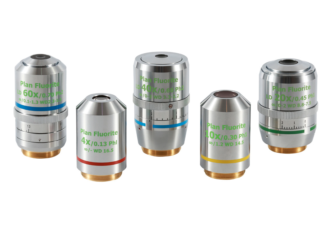
Infinity correction, bright field achromatism; 5× low magnification with low NA, yet featuring an ultra-long working distance (22.5mm), an extra-large field of view (5mm), and an extremely deep depth of focus (16.27μm), resistant to sample height differences.
Applications:
Bright field observation of large-sized, thick samples or those requiring a long operating space, such as macro surface scanning of 3D printed parts and global observation of large biological tissue sections, which can quickly cover a large range of samples.

Infinity correction, bright field achromatism; 10× magnification balanced with NA=0.30, moderate working distance, with a field of view and resolution that take both macro and micrometer-level details into account.
Applications:
Routine bright field observation, such as overall observation of cell culture dishes, inspection of small precision parts (micrometer-level scratches / structures).
Infinity correction, bright field achromatism; 20× medium-high magnification + NA=0.46, submicron resolution (0.60μm), working distance of 3.1mm, suitable for conventional samples.
Applications:
Bright field analysis of submicron-level structures, such as observation of shallow surface defects (micro-cracks, particles) in semiconductor chips and cellular substructures (distribution of organelles).

Infinity correction, bright field achromatic; 50× high magnification + NA=0.80, achieving a nanoscale resolution of 0.34μm, but with a short working distance and shallow depth of focus, requiring high sample flatness.
Applications:
Bright field observation of nanoscale fine structures, such as nanowires in semiconductor devices, microtopography of metal grain boundaries, or ultrastructural analysis of ultrathin sections.
Widely used in dynamic fluorescence imaging of living cells, multicolor fluorescence diagnosis of pathological sections, deep imaging of 3D biological structures

10x magnification, numerical aperture (NA) 0.3, ultra-long working distance (16.2mm), flat-field semi-apochromatic correction, air medium, compatible with 0.17mm cover glass, excellent wide-spectrum light transmittance.
Applications:
Suitable for large-field fluorescence observation (such as screening the fluorescence distribution of cell populations), brightfield/fluorescence multimodal switching of thick samples (such as the shallow layer of tissue sections). The long working distance can avoid damaging samples and facilitate preliminary positioning.

20x magnification, NA=0.5, working distance 2.2mm, flat-field semi-apochromatic correction, air medium, compatible with 0.17mm coverslips, balancing field of view and submicron resolution.
Applications:
For fluorescence imaging of cellular substructures (such as mitochondria, endoplasmic reticulum labeling), or multi-modal analysis (brightfield/fluorescence/DIC) of thin biological samples (single cells, ultra-thin tissues).

40x magnification, NA=0.75, working distance 0.66mm, flat field semi-apochromatic correction, air medium, with spring protection (to prevent lens-sample collision), compatible with 0.17mm cover glass.
Applications:
Suitable for fluorescence observation of submicron structures (such as the fine distribution of organelles, protein localization), or brightfield/fluorescence research on precision biological samples (such as neuronal synapses). The spring design enhances operational safety.
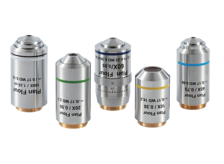
60x magnification, NA=0.85, working distance 0.3 - 0.36mm, flat-field semi-apochromatic correction, air medium, with spring protection, compatible with 0.11 - 0.23mm cover glasses (suitable for various types of preparations).
Applications:
For high-resolution fluorescence imaging (such as nuclear chromatin, small particle markers), adaptable to special samples with different cover glass thicknesses (such as custom sections), and spring protection ensures operational safety.

100x magnification, NA=1.35, working distance 0.16mm, flat-field semi-apochromatic correction, oil immersion medium (enhancing light gathering and resolution), with spring protection, compatible with 0.17mm cover slips, and excellent wide-spectrum light transmittance.
Applications:
Suitable for fluorescence observation of nanoscale fine structures (such as viral particles, protein clusters, single-molecule fluorescence), or extreme-resolution imaging of chromosomes and organelle ultrastructures. Oil immersion can significantly improve signal brightness and resolution.
Widely used in multimodal dynamic research of living cells, cell function and toxicity analysis, fine observation of transparent/thin samples, imaging of samples in plastic containers
As a low-magnification multimodal objective lens, infinite correction + semi-apochromatic correction ensure imaging quality; the ultra-long working distance (16.5mm) provides sufficient operating space for thick samples (such as large tissue blocks, 3D cultures) and large-sized samples (global scanning of culture dishes).
Applications:
Suitable for "macro positioning + multimodal preliminary screening" (global observation in bright field, overall distribution of fluorescent labels, preliminary identification of phase-contrast samples).

"Low magnification → medium magnification" transitional objective lens, with balanced NA and magnification; the working distance is still long (14.5mm), taking into account both large field of view and resolution.
Applications:
It can be used for screening the fluorescence distribution of cell populations, phase contrast observation in the early stage of living cell division, or rapid switching analysis of "bright field → fluorescence" for thin tissues.

Medium-magnification high-precision imaging objective lens, with improved NA achieving "submicron-level resolution"; the correction collar solves the aberration problem caused by uneven thickness of cover slips/samples, adapting to various preparations; moderate working distance.
Applications:
Suitable for fluorescence labeling observation of cellular substructures (mitochondria, endoplasmic reticulum), or phase contrast dynamic analysis of transparent living cells (such as cell migration, morphological changes).

High-magnification submicrostructure observation objective lens with NA=0.6 ensures high resolution; correction collar + wide coverslip adaptability, compatible with different preparations; working distance (2.3–3.3mm) still provides operating space under high magnification.
Applications:
It can be used for the fine distribution of organelles (such as Golgi apparatus localization), subcellular localization of protein fluorescent labels, or phase contrast observation of neuronal synapses.

High-magnification high-precision imaging objective lens (air medium), NA=0.7, close to the performance of oil immersion lenses (no need for immersion oil); the correction ring ensures the imaging quality of thick cover slips/samples, and the working distance can meet the requirements of nuclear chromatin.
Applications:
High-resolution observation of small particle fluorescent markers (such as virus-like particles), or phase contrast analysis of ultrastructures in thin sections, providing a solution for "high-magnification imaging without oil immersion lenses".
Widely used in basic life science research, medical research and drug development, cutting-edge technologies and interdisciplinary applications

Low-magnification macroscopic observation objective lens with apochromatic correction to ensure color accuracy, and an ultra-long working distance of 8.5mm, suitable for thick samples and large containers.
Applications:
Suitable for brightfield/fluorescence "pre-positioning" (quickly finding the target area to lay the foundation for high-magnification observation).

Apochromatic correction ensures true colors. 4× low magnification + 20mm ultra-long working distance (large field of view, easy to operate). Air medium, no need for immersion liquid or specific cover slips, simple and flexible.
Applications:
Suitable for global observation of thick samples, such as the overall morphology and distribution observation of large tissue blocks, 3D cell clusters (organoids), and microbial communities.

Entering the medium-magnification observation range, NA enhancement ensures the resolution leap from "cell population to substructure"; apochromatism makes fluorescent labels such as GFP and DAPI "display true colors without crosstalk".
Applications:
Suitable for "mesoscopic analysis" of cell cultures and conventional tissue sections (such as cell density statistics, observation of tissue layer structures).

A benchmark for high-resolution imaging in air medium, with NA=0.8 approaching the performance of an oil immersion lens (no immersion oil required); spring protection prevents the objective lens from crushing the sample during operation
Applications:
Suitable for "high-magnification precise observation" of dynamic live cells (such as division, migration) and fluorescently labeled organelles (mitochondria, endoplasmic reticulum).

"Quasi-oil immersion lens experience" without the need for oil immersion, high NA ensures submicron resolution; wide cover glass adaptability (0.11–0.23mm) is compatible with various preparations
Applications:
Suitable for "oil-free high-resolution observation" of cytoskeleton and nuclear details, simplifying operations while maintaining accuracy.

NA=1.42 breaks the air diffraction limit; apochromatism enables "zero error in colocalization" for multicolor fluorescence (such as DAPI+GFP+RFP)
Applications:
Suitable for high-magnification analysis of virus particles, chromatin fibers, and single-molecule fluorescent labeling.
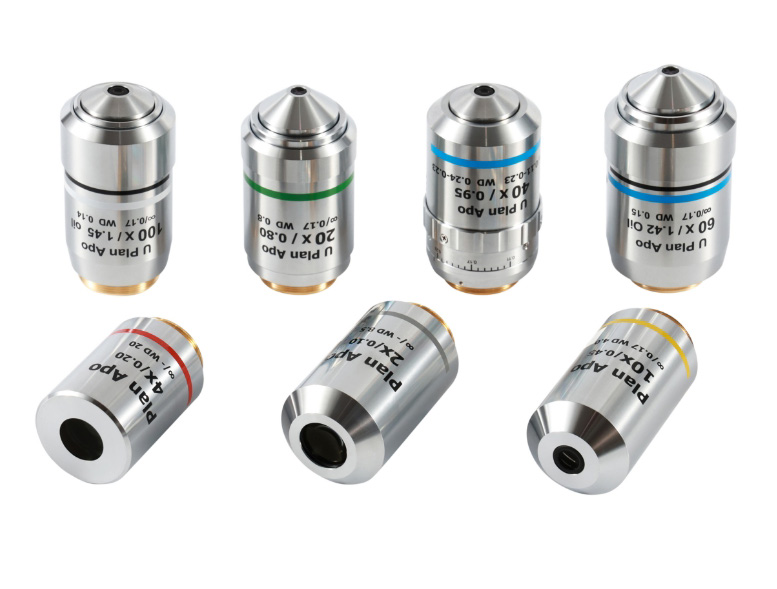
Oil immersion lens: "performance ceiling" with NA=1.45 achieving "nanoscale resolution"; apochromatic correction covering the entire chromatographic spectrum.
Applications:
The "ultimate observation tool" for cellular substructures (mitochondrial cristae, synapses), microorganisms (bacterial flagella), and immunofluorescent single-molecule localization.

