| Quantity | Price(USD) | Ship Date |
|---|---|---|
| 1-10 | TBD | |
| 10- | TBD |
NOTE : Ship Dates above are subject to change depending upon availability.
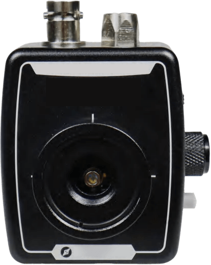
It has high spatial resolution and can accurately detect light signals in tiny areas.
It is suitable for optical inspection of tiny defects in chips during semiconductor chip manufacturing.
| Spectral Response Range | Sensitive Area Size | APD bias voltage adjustment range | APD gain M |
|---|---|---|---|
| 800~1700nm | Φ0.08mm | 0 ~ 55 V | 0 ~ 30 |
| Quantity | Price(USD) | Ship Date |
|---|---|---|
| 1-10 | TBD | |
| 10- | TBD |


