High-Throughput Wafer Metrology: An Automated Optical Workflow for Sub-Micron Defect Detection
Author: M. Chen, Senior Metrology Engineer, Semiconductor QA Division
In semiconductor manufacturing, yield is everything. Even a microscopic scratch, a residual photoresist flake, or a stray particulate on a silicon wafer can compromise dozens of dies, costing thousands of dollars. As our fabrication nodes shrink, relying on manual inspection for quality control has become a bottleneck, leading to operator fatigue and inconsistent defect classification.
To maintain strict quality control without sacrificing production speed, our cleanroom implemented a fully automated, high-resolution optical inspection workflow. Here is a breakdown of the system architecture we use to scan, map, and classify sub-micron surface defects across entire wafers.
1. The Reflective Optical Path
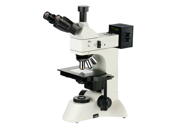
Unlike biological samples, silicon wafers and semiconductor materials are completely opaque. Transmitted light is useless here. We built our inspection station around a VenusLab U-Met Metallurgical Microscope — an upright, episcopic optical system that directs light down through the objective lens and measures the light reflected back from the wafer surface. The robust stand provides the extreme vibration isolation required when magnifying surface features up to 1000x in a busy fab environment.
2. Revealing Topography with Advanced Illumination
The secret to finding nearly invisible defects on a highly reflective mirror-like surface is controlling how light hits it. We integrated a Fiber-Coupled LED system for its highly stable, high-intensity output and rapid switching between inspection modes.
- We use Brightfield (BF) to check for color variations, film thickness uniformity, and larger structural flaws.
- However, the real workhorse is Darkfield (DF) illumination. By directing light at an oblique angle, the flat mirror surface appears pitch black, while any raised particle, scratch, or edge defect brilliantly scatters the light, making it stand out instantly.
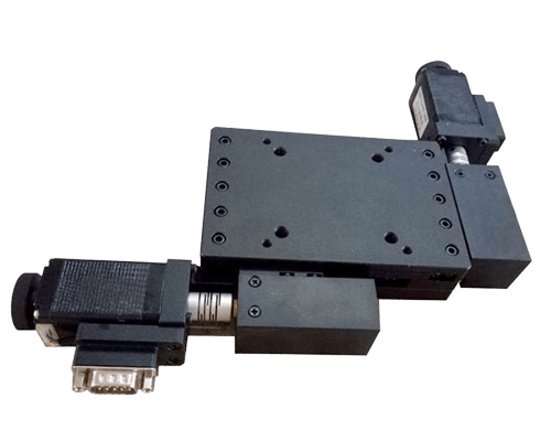
3. Navigating the Wafer Map
Scanning an entire 8-inch or 12-inch wafer at high magnification requires covering thousands of individual fields of view. We cannot afford manual stage adjustments. Our system is driven by a VL Integrated XY Stage — a high-precision motorized positioning platform that we program directly with the wafer map. The stage systematically steps across the grid with sub-micron repeatability, ensuring 100% surface coverage and allowing us to assign exact X-Y coordinates to every detected flaw for downstream review.
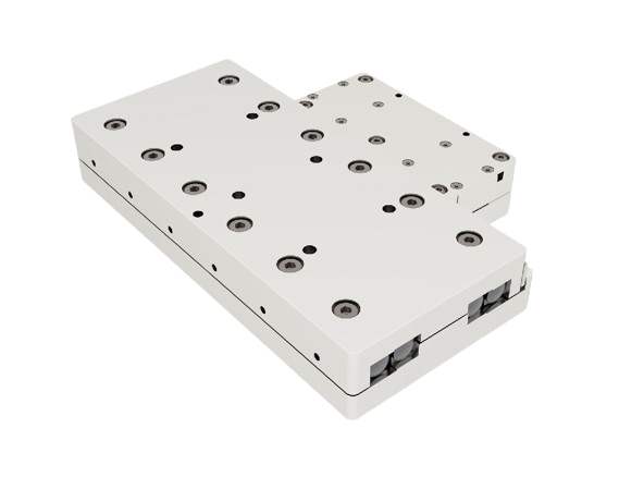
4. Compensating for Nanoscale Warpage
At high magnifications, the depth of field is incredibly shallow. Even the highest quality wafers have slight bow or warpage, meaning the surface will naturally drift out of focus as the stage moves from the center to the edge. To keep the scanning process running at maximum speed without pausing to refocus manually, we mounted the objective lenses on VenusLab Piezo Z-axis actuators. These ultra-fast, high-resolution devices provide real-time, nanometer-level Z-axis corrections, ensuring every acquired image is perfectly sharp.
5. High-Speed Image Acquisition
To maintain high throughput, the camera must capture images without requiring the motorized stage to come to a complete stop — a technique called "fly-by" scanning. For this we deployed the Venuslab-ISP CMOS Camera series, which features global shutters across its lineup. Unlike rolling shutters that can warp moving objects, the global shutter freezes the motion perfectly. The high pixel count allows us to resolve sub-micron defects across a large field of view, drastically reducing the total number of images needed to map the entire wafer.
Conclusion
By combining the reflective optics of a metallurgical microscope with high-speed motorized XY scanning, dynamic piezo autofocus, and dual brightfield/darkfield LED illumination, we eliminated the bottleneck in our QA process. This automated workflow allows us to detect, classify, and map critical defects in a fraction of the time, directly contributing to a higher overall die yield.