| Quantity | Price(USD) | Ship Date |
|---|---|---|
| 1-10 | TBD | |
| 10- | TBD |
NOTE : Ship Dates above are subject to change depending upon availability.

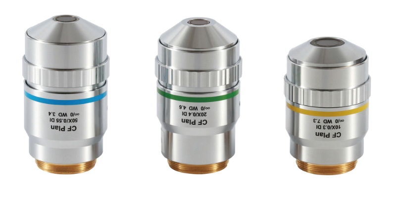
A low numerical aperture (0.3) ensures a large field of view, a long working distance adapts to thick samples or operating spaces, and a large depth of focus tolerates surface height differences, making it suitable for three-dimensional topography analysis of rough surfaces.
Applied to:
Global defect scanning of semiconductor wafers (300mm) (such as scratches, particles)
Surface roughness measurement of 3D printed metal parts (large depth of focus, adapting to the height difference of layered structures)
Observation of the layered structure of thick polymer films (long working distance to avoid sample collision).
| NA | 0.3 | WD | 7.3mm |
| R | 0.92um | ±D.F | 3.05um |
| Quantity | Price(USD) | Ship Date |
|---|---|---|
| 1-10 | TBD | |
| 10- | TBD |