| Quantity | Price(USD) | Ship Date |
|---|---|---|
| 1-10 | TBD | |
| 10- | TBD |
NOTE : Ship Dates above are subject to change depending upon availability.

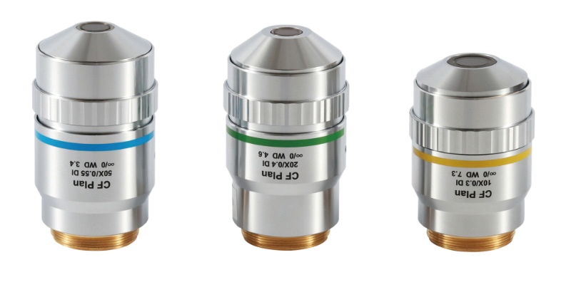
Balanced medium magnification and NA, resolution adapted to submicron structures, moderate working distance, and depth of field matching moderately rough surfaces.
Applications include:
Measurement of geometric features of chip pads (such as solder ball height and spacing);
Observation of wrinkles and grain boundaries in graphene/molybdenum disulfide (MoS₂) (contrast enhanced by DI technology);
Detection of micro-defects in small mechanical parts (such as flash and cracks in injection-molded parts).
| NA | 0.4 | WD | 4.6mm |
| R | 0.69um | ±D.F | 1.72um |
| Quantity | Price(USD) | Ship Date |
|---|---|---|
| 1-10 | TBD | |
| 10- | TBD |