| Quantity | Price(USD) | Ship Date |
|---|---|---|
| 1-10 | TBD | |
| 10- | TBD |
NOTE : Ship Dates above are subject to change depending upon availability.

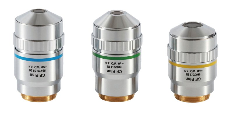
A high NA (0.55) improves the resolution to 0.50μm, enabling observation of nanostructures; a small depth of focus is suitable for high-precision measurement of flat surfaces.
Applications include:
Nanoscale scratch/short circuit detection of semiconductor chips (with a resolution of 0.50μm, suitable for nanoscale defects);
Analysis of atomic arrangement and defects in metal grain boundaries (DI technology enhances grain boundary contrast);
Precise 3D topography measurement of MEMS devices (such as bending deformation of microbeams).
| NA | 0.55 | WD | 3.4mm |
| R | 0.50um | ±D.F | 0.91um |
| Quantity | Price(USD) | Ship Date |
|---|---|---|
| 1-10 | TBD | |
| 10- | TBD |