| Quantity | Price(USD) | Ship Date |
|---|---|---|
| 1-10 | TBD | |
| 10- | TBD |
NOTE : Ship Dates above are subject to change depending upon availability.

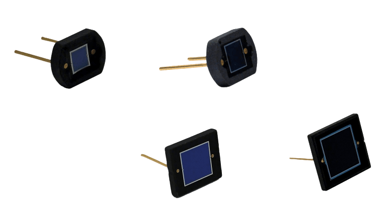
Designed with the largest photosensitive surface, it can cover an ultra-large detection area without the need for multi-chip splicing. It is suitable for detecting strong light and large-area optical signals, and reduces the complexity of the optical system inside the device.
It is suitable for optical power density monitoring of large-scale ultraviolet curing equipment (such as curing of wide-format plastic parts) and industrial-grade large-area strong light detection terminals, matching high-power scenarios of "optical power detection".
| Photosensitive Area Size (mm) | 10×10 | Window Material | Resin |
| Spectral Response Range (nm) | 320~1060 | Dark Current (Max, pA) | 800 |
| Junction Capacitance (Max, pF) | 1000 | Equivalent Noise Power (W/Hz¹/²) | 1.2×10⁻¹⁴ |
| Quantity | Price(USD) | Ship Date |
|---|---|---|
| 1-10 | TBD | |
| 10- | TBD |