| Quantity | Price(USD) | Ship Date |
|---|---|---|
| 1-10 | TBD | |
| 10- | TBD |
NOTE : Ship Dates above are subject to change depending upon availability.

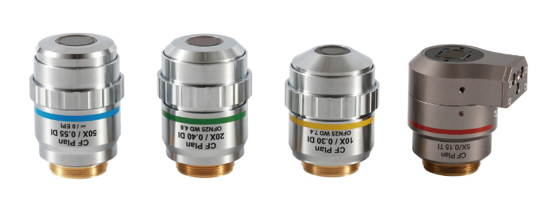
The magnification and numerical aperture are balanced, with resolution suitable for submicron-level structures, moderate depth of focus, and compatibility with surfaces of medium roughness.
Applications:
It can be used for measuring the geometric features (height, spacing) of semiconductor chip pads, or for observing wrinkles and grain boundaries in two-dimensional materials such as graphene and MoS₂ (DI technology enhances structural contrast).
| NA | 0.3 | WD | 7.4mm |
| R | 0.92um | ±D.F | 3.06um |
| Quantity | Price(USD) | Ship Date |
|---|---|---|
| 1-10 | TBD | |
| 10- | TBD |