| Quantity | Price(USD) | Ship Date |
|---|---|---|
| 1-10 | TBD | |
| 10- | TBD |
NOTE : Ship Dates above are subject to change depending upon availability.
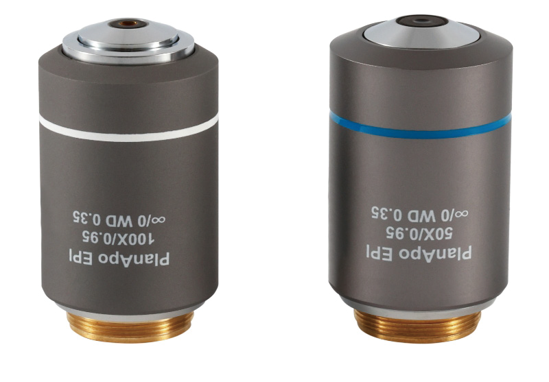
It adopts apochromatic correction (achromatism in the entire visible light range of 400–700nm) and flat-field design to eliminate field curvature and color fringing interference. At 50× magnification, it balances resolution and field of view, making it suitable for fine observation at medium magnification.
Applications:
Defect detection of semiconductor chip solder joints (balancing field of view and resolution), analysis of metal grain distribution, and observation of wear at medium magnification for precision molds.
| NA | WD | R | ±D.F |
|---|---|---|---|
| 0.95 | 0.35mm | 0.29um | 0.3um |
| Quantity | Price(USD) | Ship Date |
|---|---|---|
| 1-10 | TBD | |
| 10- | TBD |


