| Quantity | Price(USD) | Ship Date |
|---|---|---|
| 1-10 | TBD | |
| 10- | TBD |
NOTE : Ship Dates above are subject to change depending upon availability.
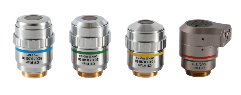
Further improve the resolution at medium and high magnifications to adapt to finer sub-micron structures, and balance the working distance and depth of field.
Applications:
Suitable for 3D topography detection of MEMS devices (such as microbeams, microvalves), or microscopic analysis of grain boundaries in metal materials (observing atomic arrangement distortions).
| NA | WD | R | ±D.F |
|---|---|---|---|
| 0.4 | 4.6mm | 0.69um | 1.72um |
| Quantity | Price(USD) | Ship Date |
|---|---|---|
| 1-10 | TBD | |
| 10- | TBD |


