Widely used in fields such as semiconductors (wafer defects / film thickness), optical components (surface flatness), precision manufacturing (part roughness)
• Nanoscale non-contact precision • Serial scene adaptation • Industry universal benchmark
Download
Data Sheet
Overview
Introduction:
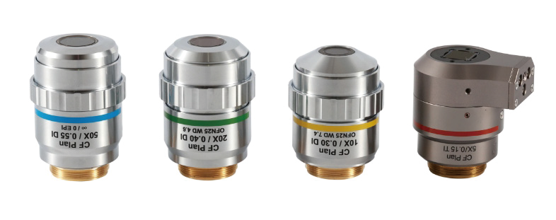
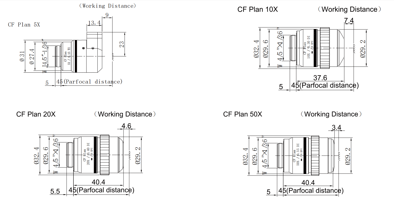
Infinite conjugate
45mm parfocal
Non-contact measurement of surface topography and geometric features