Product image
Product image

Near-infrared enhanced silicon PIN photodiode (DIP package)

A passive photoelectric conversion functional device with a dual in-line package (DIP) through-hole package.

  • Accurately capture weak signals
  • Low dark current + high linearity
  • Strong environmental adaptability + low-cost maintenance
Download
Data Sheet

Overview

Introduction:

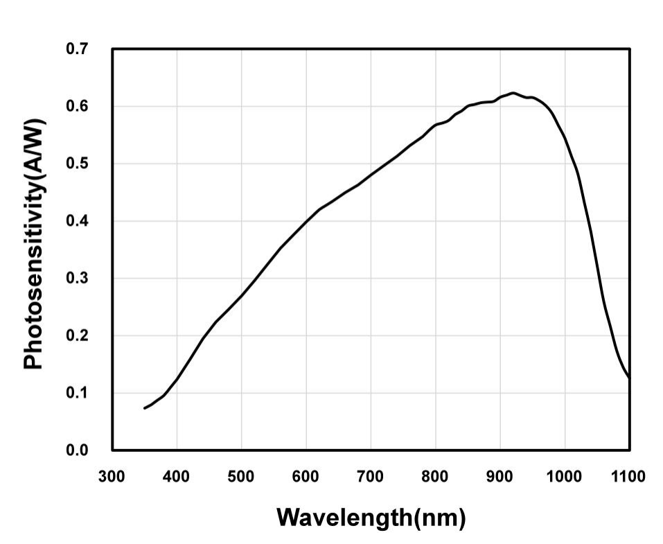
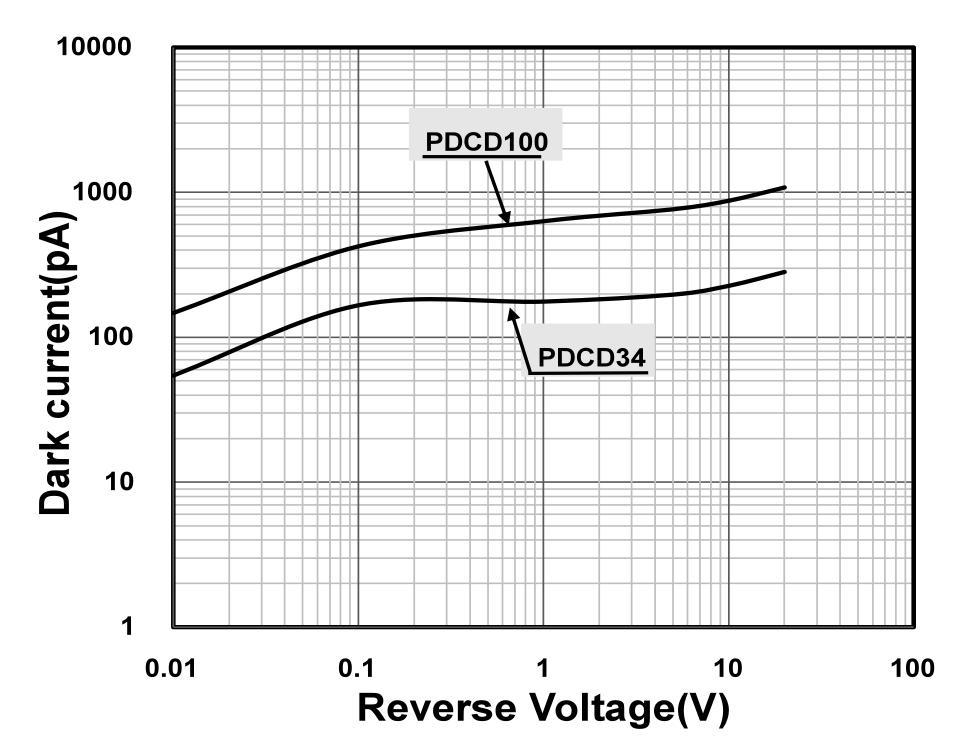
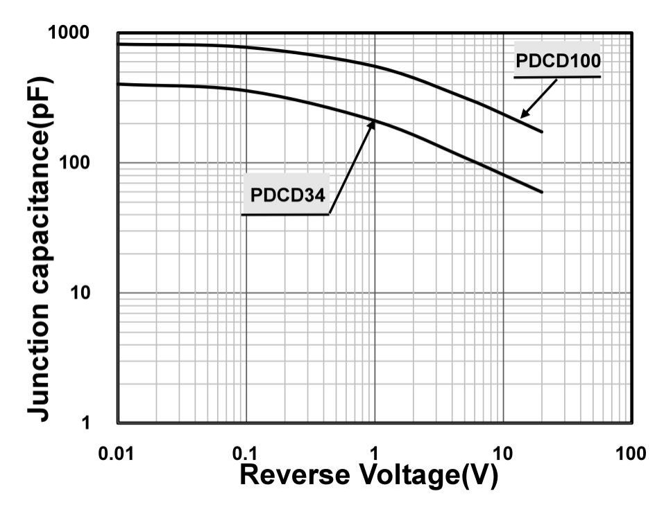
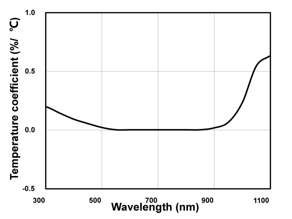
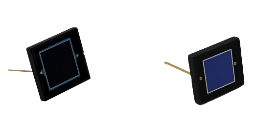
This device has a spectral response range of 350~1100nm, with optimized response for near-infrared wavelengths, and features low dark current. It is suitable for photoelectric measurement instruments, optical analysis equipment, and optical power monitoring scenarios.


It can adapt to anti-interference, high-speed, and low-power consumption scenarios without the need for additional peripheral chips, and can also simplify circuit design and reduce the overall solution cost.


Features:


  • With a silicon-based PIN structure as the core
  • Equipped with a highly transparent photosensitive window
  • Wide range of applicable operating voltages
  • With photocurrent as the main output form


Dimension:


Specifcations

Applications

Serivce & Support

Explore Series

Model
Photosensitive Area Size
Maximum Dark Current (ID, VR=0V)
Junction Capacitance (Cj, VR=10mV)
Noise Equivalent Power (NEP)
Rise Time (tr)
Peak Responsivity Wavelength & Photoresponse
Action
Telegram LogoWhatsApp Logo