Near-infrared enhanced silicon PIN photodiode (DIP package)

Product image
Product image

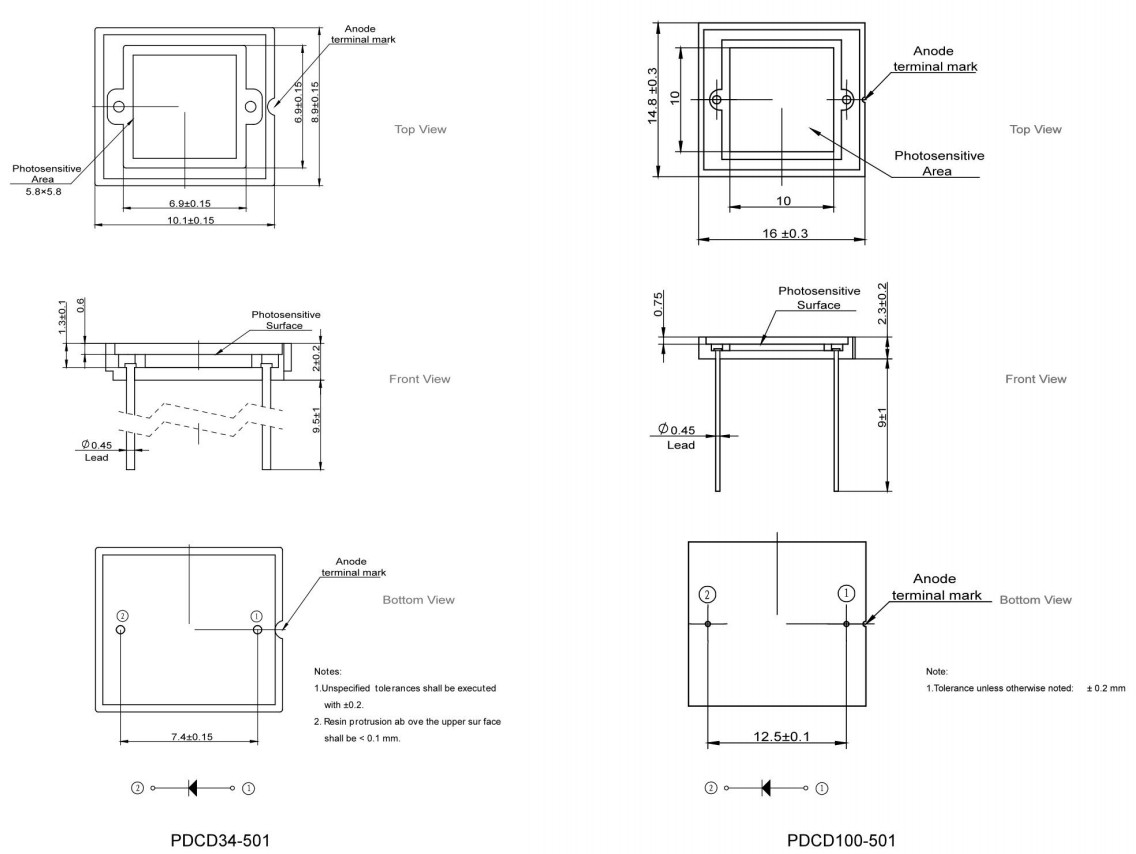
采用双列直插(DIP)通孔封装的被动式光电转换功能器件。

  • 精准捕捉弱信号
  • 低暗电流 + 高线性度
  • 强环境适配 + 低成本维护


输入您的电子邮件地址可免费访问、接收产品手册或享受特别折扣。
Overview
Specifcations
Applications

Introduction:

This device has a spectral response range of 350~1100nm, with optimized response for near-infrared wavelengths, and features low dark current. It is suitable for photoelectric measurement instruments, optical analysis equipment, and optical power monitoring scenarios.


It can adapt to anti-interference, high-speed, and low-power consumption scenarios without the need for additional peripheral chips, and can also simplify circuit design and reduce the overall solution cost.


Features:


  • With a silicon-based PIN structure as the core
  • Equipped with a highly transparent photosensitive window
  • Wide range of applicable operating voltages
  • With photocurrent as the main output form


Dimension:


浏览全部型号

Near-infrared enhanced silicon PIN photodiode (DIP package)

PDCD34-501
The size of the photosensitive surface is 5.8×5.8 mm, and it has high near-infrared detection efficiency.
最快发货 同一天
库存物品包含

Near-infrared enhanced silicon PIN photodiode (DIP package)

PDCD100-501
The photosensitive area size is 10×10mm, and it has high near-infrared detection efficiency.
最快发货 同一天
库存物品包含
Telegram LogoWhatsApp Logo