订阅Venus Lab Inner Lens,抢先获得行业最新
科研突破、新品发布和特别活动的独家内幕。
当订阅我们的品牌资讯时,您的个人信息将被妥善保护,
并严格遵守我们的隐私政策。

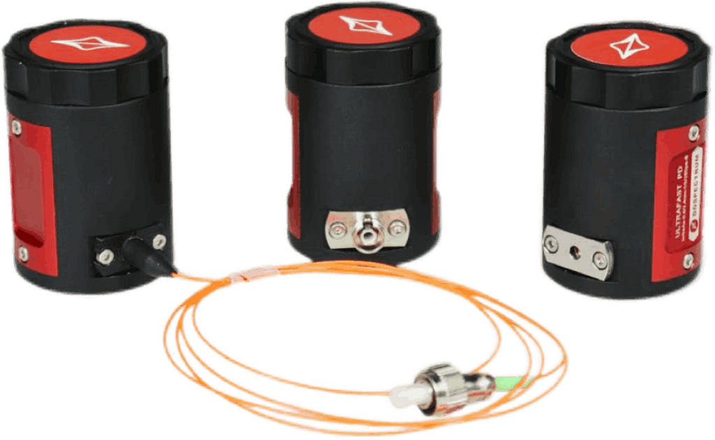
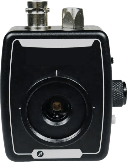
覆盖 EUV 光源稳定性监测(中等面积均匀采集)、科研光谱仪模块(适配标准光阑尺寸);可见光失明特性避免杂光干扰,可调增益灵活匹配实验室级动态信号范围(弱光→中强光)。

适用于 EUV 光刻曝光剂量监测(大面积均匀测辐)、等离子体诊断(捕获瞬态强辐射);SiC 耐高通量辐照特性保障长寿命,8 档增益覆盖从 “弱信号解析” 到 “强脉冲量化” 的全场景。

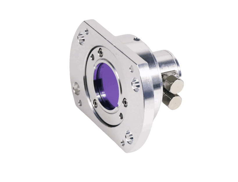
适配 EUV 光源远场分布测试(广域覆盖低照度信号)、大面积镀膜均匀性检测(单次扫描覆盖更大区域);真空法兰支持高真空腔集成,可调增益在 “广域弱光” 与 “局部强光” 间无缝切换,突破传统探测器动态范围瓶颈。

适配 VUV 光刻掩膜纳米缺陷检测(捕捉亚微米级缺陷信号)、单分子层表面分析(高分辨率解析 VUV 光与超薄样品的相互作用);依托 SiC 基低暗电流特性,8 档增益精准放大极弱 VUV 信号,真空法兰兼容≤10⁻⁴Pa 高真空环境,保障超高精度测量不受杂气干扰。

覆盖 科研级 VUV 光谱仪模块(适配标准光阑尺寸,兼顾信号强度与分辨率)、VUV 光源稳定性监测(中等面积均匀采集,保障数据代表性);可见光失明特性消除环境杂光干扰,可调增益灵活匹配实验室级动态信号范围(弱光→中强光),满足多场景测试需求。

适用于 VUV 镀膜均匀性检测(单次扫描覆盖典型区域,快速评估膜层质量)、等离子体瞬态辐射诊断(捕捉毫秒级 VUV 脉冲信号);SiC 耐高通量 VUV 辐照特性保障长寿命,8 档增益覆盖从 “弱信号解析” 到 “强脉冲量化” 的全场景,真空法兰支持高真空腔集成。

适配 大面积薄膜沉积监测(宽幅覆盖,高效检测膜层均匀性)、VUV 等离子体广域诊断(单探测器覆盖更大空间范围,减少扫描次数);SiC 基高稳定性与耐辐照性能保障长期可靠运行,可调增益在 “弱光信号” 与 “强辐射脉冲” 间无缝切换,真空法兰兼容高真空环境(≤10⁻⁴Pa)。

适用于 VUV 光源远场分布测试(广域覆盖低照度信号,还原光源空间分布特性)、大面积涂层均匀性检测(单次扫描覆盖超大区域,提升检测效率);真空法兰支持高真空腔集成,可调增益突破传统探测器动态范围瓶颈,在 “广域弱光” 与 “局部强光” 间灵活切换,满足复杂场景测试需求。
聚焦工业级与科研级中紫外波段精准测量需求
材质赋能高稳定性
信号纯净抗干扰
增益灵活全场景适配
多场景兼容设计
长效可靠低维护
Mid-UV general model (220–350nm), φ1mm circular aperture balances resolution and light flux.
8-level 0–70dB gain suits all light intensities. Ideal for light source spectral calibration, UV curing oven monitoring.

Micro-region detector (220–350nm), 0.5×0.5mm square (φ0.25mm equivalent) enables micron-level resolution for local signals.
Suits chip UV damage localization, lithography mask defect imaging.

Wide-area long-life model (220–350nm), 2×2mm square (φ4mm equivalent) + “-L” radiation resistance. Suits fusion UV monitoring, strong light source aging tests.
Wide-area strong-light model (220–350nm), 2×2mm square (φ4mm equivalent) without long-life reinforcement. High responsivity (@300nm: 0.9A/W).
Suits coating uniformity inspection, light source far-field mapping.

Long-wave extended model (225–380nm), φ1mm circle covers near-UV (365nm). High responsivity (@285nm: 1.27A/W).
Suits 365nm curing light monitoring, near-UV material testing.

Deep-UV general model (220–280nm), φ1mm circle focuses on short waves. Precise response (@265nm).
Suits 254nm disinfection lamp irradiance quantification, lithography dose monitoring.

Deep-UV micro-region model (220–280nm), 0.5×0.5mm square (φ0.25mm equivalent). Dual precision of short waves + micro-regions.
Suits photoresist micro-defects, chip etching damage localization.
Optoelectronic devices based on wide bandgap semiconductors.

It balances the photosensitive area and resolution, adapting to most ultraviolet detection scenarios; it has a wide gain range, supporting signal conversion from weak light (nW level) to strong light (μW level).
Applications: Laboratory ultraviolet spectroscopy analysis, UV curing equipment light intensity monitoring, miniaturized ultraviolet sensing modules.

It has extremely high spatial resolution and can detect ultraviolet light in tiny areas; its small size is suitable for high-density integrated devices.
Applications: UV lithography monitoring of semiconductor wafers, spot analysis of micro UV lasers, UV excitation light detection of biochips.

It has a large single detection area and is suitable for scattered ultraviolet light (such as greenhouse UVB radiation, large-area UV coating curing monitoring); the large size improves light collection efficiency.
Applications: UV radiation monitoring in agricultural greenhouses, large-area light intensity distribution testing of UV sterilization lamps, and light power detection of large UV curing ovens.

It has an outstanding response to long-wave ultraviolet rays and is suitable for UVA band detection; it is compatible with the visible light and near-ultraviolet regions in a wide band.
Applications: Cosmetics UVA/UVB protection testing, fluorescence excitation (405nm laser), long-wave ultraviolet germicidal lamp monitoring.
Short-wave ultraviolet has strong selectivity and is suitable for scenarios where long-wave interference needs to be excluded; small size improves spatial resolution.
Applications: Biomedical deep ultraviolet imaging, semiconductor deep ultraviolet lithography detection, 325nm laser power calibration.

Highly efficient deep ultraviolet response, suitable for high-energy short-wave ultraviolet detection; high sensitivity to capture weak deep ultraviolet signals.
Applications: Light intensity monitoring of medical UVC disinfection equipment, quality inspection of deep ultraviolet LEDs, evaluation of ultraviolet sterilization effect.

Covers a wide band of ultraviolet + visible light near-ultraviolet regions, suitable for multi-wavelength detection; strong compatibility, reducing equipment replacement costs.
Applications: multispectral ultraviolet analyzers, color fluorescence microscopes, performance testing of wide-band ultraviolet lamps (290~440nm).
A dedicated radiation measurement device designed based on silicon (Si) material.

This model has strong spatial adaptability. Its compact appearance and small photosensitive area make it suitable for integration into devices with limited space. Moreover, it has low interference and high stability. The low junction capacitance of 25pF (when VR=100V) can reduce high-frequency signal interference.
Applications: Small-scale synchrotron radiation experiments, flaw detection of small-sized semiconductors/metal parts, and integration into portable radiation detectors.

This model is suitable for distributed radiation fields to reduce detection blind areas and can capture rapidly changing radiation signals.
The aluminum-plated photosensitive surface can filter out interference in the ultraviolet band, eliminating the need for additional filters, making it suitable for open-air or strong background light environments.
Constructed based on indium arsenide antimonide (InAsSb) material

It is sensitive to the visible light band, has low noise, controllable cost, and strong integration (compatible with SMA interface and M4 support rod).
Applications: Visible light high-speed laser pulse waveform measurement, desktop-level quantum physics experiments.

Large photosensitive surface adapts to "wide light field" visible light detection, with low cost, meeting the needs of medium and low-speed scenarios.
Applications: Medium and low-speed visible light signal monitoring, teaching demonstration experiments.

Near-infrared "large light field" detection, suitable for weak signal or large-area light field scenarios.
Applications: Near-infrared weak signal measurement, large-area light field distribution monitoring.

Near-infrared "medium-speed" response, with a moderately sized photosensitive surface (balancing detection efficiency and accuracy).
Applications: Near-infrared medium-speed laser pulse detection, online monitoring of industrial production lines.
Near-infrared "high-speed" response, and small photosensitive surface enables "precise light field" detection.
Applications: Demodulation of near-infrared high-speed optical communication signals, precision measurement in scientific research.

Near-infrared "ultra-high speed + ultra-high bandwidth" with an extremely small photosensitive surface to accurately capture extremely short light pulses.
Applications: Near-infrared pulse demodulation in quantum communication, real-time signal capture in near-infrared lidar.

"Cross-band" coverage (visible light + near-infrared), with a large photosensitive surface suitable for multiple scenarios.
Applications: synchronous monitoring of multi-band optical signals, environmental spectral analysis.

"Long near-infrared" exclusive detection, with a large photosensitive surface adapted to long-wave scenarios.
Applications: Long-wave near-infrared gas detection (such as methane), infrared composition analysis of materials.

"Mid-infrared" band detection fills the gap in long-wave.
Applications: mid-infrared spectral analysis, deep space infrared signal detection.
Silicon-based amplifying photodetector

It has strong parameter balance, wide adaptability in terms of photosensitive range, response speed, and target surface size, without the need to compromise for a single scenario.
High bandwidth combined with fast response can accurately capture high-speed optical signals, reducing signal delay and distortion.
It has high ultraviolet response sensitivity and can stably capture 190nm short-wave ultraviolet light signals. It is suitable for measuring small ultraviolet light spots after focusing with medium and small target surfaces, avoiding stray light interference introduced by large target surfaces.
It maintains the same gain adjustment logic as other models in the same series, ensuring consistent operating habits and reducing the cost of switching between multiple devices.

The large target surface design can receive light signals over a larger area, avoiding the "cutting" of large light spots by small target surfaces, making it suitable for surface light source detection. With a response time of 35ns, it balances the needs of a large target surface and medium-to-high speed requirements.
It has no ultraviolet enhancement design, so its cost is lower than that of ultraviolet models. It is suitable for large light spot scenarios with pure visible light/near-infrared, offering higher cost performance.

The only "ultraviolet enhancement + large target surface" combined model can not only capture 190nm ultraviolet light, but also receive large light spot signals, adapting to complex and multi-demand scenarios.
The large target surface reduces the missed capture of large light spot signals, and combined with ultraviolet enhancement, it can be used for global light intensity measurement of ultraviolet large-area light sources.
It can directly replace imported large target surface ultraviolet detectors, reducing the cost of equipment upgrading.
Optoelectronic devices designed for the near-infrared band (800~1700nm)

Seamlessly compatible with Thorlabs devices, with low replacement costs.
High-speed response + high bandwidth, suitable for rapid optical signal capture.

Medium-speed response is suitable for most conventional scenarios, balancing speed and stability.
Application: Medium-speed near-infrared light intensity monitoring (such as optical signal feedback in industrial laser processing).

A large target surface is compatible with small and medium-sized light spots, avoiding signal missed capture.
Application: Near-infrared detection of small, medium and large light spots (such as near-infrared spectroscopy analysis).
A larger target surface is suitable for medium and large light spots, with stronger low-light capturing capability.
Application: Near-infrared measurement of medium and large light spots (such as lidar signal reception).

Low-speed response adapts to low-light scenarios with high signal stability.
Application: Low-speed, low-light near-infrared detection (such as weak signal detection of trace gases).

The target surface is the largest, suitable for ultra-large light spots, and has good low-light integration effect.
Application: Ultra-large light spot near-infrared monitoring (such as surface light source near-infrared light intensity distribution testing).
Optoelectronic devices with indium gallium arsenide (InGaAs) as the core detection material
Seamlessly compatible with Thorlabs devices, with low replacement costs.
High-speed response + high bandwidth, suitable for fast optical signal capture.

The large target surface design reduces the risk of missing large light spot signals, is suitable for surface light sources or divergent light detection, and has strong compatibility.
Applications: Near and mid-infrared large light spot detection (such as near-infrared light intensity distribution testing of surface light sources, transmittance calibration of large-aperture optical components).

The infrared extends to 2600nm, covering the near to mid-infrared bands, with high sensitivity for weak light detection (low NEP).
Applications: Mid-infrared weak light detection (such as capturing mid-infrared absorption signals of gases in TDLAS technology, mid-infrared spectral analysis).

It has both "infrared extension + large target surface", is suitable for mid-infrared large light spot scenarios, and has good low-light integration effect.
Applications: Mid-infrared large light spot measurement (such as mid-infrared surface light source intensity monitoring, performance testing of large-size mid-infrared optical components).
An amplifying optoelectronic device made of silicon as the detection material, specially designed for the ultraviolet to visible light band.

High-speed response + medium to high bandwidth, fast capture speed for weak light signals, and parameters suitable for most conventional fast scenarios.
Application: Fast weak light measurement (such as laser pulse intensity monitoring).
Covers both ultraviolet and visible light dual bands, with high bandwidth to adapt to ultra-high-speed signals and strong low-light amplification capability.
Application: High-speed detection of ultraviolet + visible light (such as light intensity calibration of ultraviolet disinfection equipment).

High bandwidth + high gain, stable signal conversion in the visible light band, no need for ultraviolet adaptation costs.
Application: High-speed visible light optoelectronic development (such as pre-stage signal conversion for industrial visible light imaging).

The noise equivalent power (NEP) is as low as 3.0×10⁻¹⁵ W/Hz¹/², with outstanding detection capability for extremely weak light (fW level).
Applications: Measurement of extremely weak light signals (such as low-light imaging, weak signal capture in trace gas detection).

Gain and bandwidth parameters are balanced, suitable for most non-extreme scenarios, achieving a balance between cost and performance.
Application: General visible light photodetection (such as routine light intensity measurement in laboratories).
Ear-infrared dedicated detection equipment
It balances high bandwidth and medium gain, with a fast capture speed for weak light signals, and has strong adaptability in conventional high-speed near-infrared scenarios.
Application: Near-infrared rapid weak light measurement (such as LiDAR near-infrared pulse signal detection).

It has outstanding ultra-high-speed signal response capability, with a balanced combination of gain and bandwidth, and can efficiently convert high-speed near-infrared optical signals.
Application: Near-infrared ultra-high-speed optoelectronic development (such as near-infrared high-speed signal reception in optical communication)

It has strong detection capability for extremely weak light (fW level) and is suitable for low-light-intensity signal scenarios.
Applications: Measurement of near-infrared extremely weak light (such as near-infrared fluorescence lifetime testing, capture of weak signals in trace gas detection).

The large target surface design is suitable for large light spot near-infrared signals. The high gain can amplify weak large light spot optical signals, and it has strong stability.
Application: Near-infrared large light spot weak light detection (such as large light spot sample signal conversion in near-infrared spectroscopy analysis).

Its infrared extension characteristics cover the mid- and near-infrared bands, which can meet the needs of cross-band detection, with balanced parameters and wide adaptability.
Application: Mid- and near-infrared cross-band detection (such as testing the spectral characteristics of mid- and near-infrared materials).
Low-cost, high-stability general-purpose photoelectric conversion devices

Its fast response capability enables it to timely capture rapidly changing optical signals, and the characteristic of visible light extension makes it applicable to various optical signal scenarios.
It performs excellently in visible light detection scenarios where high response speed is required.

It has a relatively wide range of applications and can meet various conventional light detection needs. Its low-cost feature makes it competitive in large-scale applications or cost-sensitive projects.
Applications: It can be used for light signal detection with not extremely high precision requirements on industrial production lines, such as optical detection of appearance defects of ordinary products, or basic optical experiments in educational and scientific research institutions.

A larger photosensitive size enables it to collect more light signals, resulting in better adaptability to scenarios with weak light signals or requiring large-area detection, and it can improve the sensitivity and reliability of detection.
Applications: Suitable for light signal detection in low-light environments, such as the detection of faint starlight in astronomical observations, or scenarios involving large-area light intensity distribution detection.
It can detect light signals in a wider infrared band and has strong detection capability for infrared light signals.
It also performs well in terms of response speed and bandwidth, and can meet the requirements of some high-speed scenarios that have demands for infrared light detection.

A wide infrared sensing range can cover the detection needs of more infrared light signals, and the moderate sensing size balances a certain level of light collection capability and response characteristics.
It is used in scenarios that have certain requirements for infrared light detection, such as infrared night vision detection in security monitoring, or infrared temperature monitoring in industrial production.
Silicon-based biased high-speed photoelectric conversion device
It has fast response and high bandwidth, and the window coupling is compatible with conventional optical systems.
It is suitable for general optical detection scenarios in visible light and near-infrared regions that require high response speed and bandwidth, such as signal acquisition in basic optical experiments.

Fast response, high bandwidth, and ball lens coupling enhance light collection capability.
It is used for visible light and near-infrared detection in low-light environments, such as signal detection in low-light imaging systems.

It features fast response and high bandwidth. Fiber coupling facilitates the integration of optical communication and other optical fiber systems.
It is suitable for visible light and near-infrared signal detection scenarios based on optical fibers, such as optical fiber communication and optical fiber sensing.

It has fast response and high bandwidth. The fiber coupling is compatible with fiber optic systems, and the performance is stable.
It can be used for signal detection in fields such as fiber optic communication and fiber optic sensing that have high requirements for stability.

Fiber optic coupling is suitable for fiber optic systems and has advantages in scenarios where costs are a concern or where requirements for response speed and bandwidth are relatively low.
It is applicable to detection scenarios of visible light and near-infrared fiber optic systems that require fiber coupling, with relatively loose requirements for response speed and bandwidth, such as entry-level fiber optic sensing experiments.
Silicon-based amplifying adjustable gain photodetection equipment

A large target surface is beneficial for capturing large-area weak light signals, and the 8-level adjustable gain enhances adaptability.
It is suitable for large-area low-light imaging, such as large-area imaging of tissue fluorescence in biomedicine.

It can detect ultraviolet light, with a wider range of application scenarios, and its gain is adjustable to cope with different light intensities.
It is used in scenarios such as environmental monitoring and scientific research experiments that require ultraviolet light detection, such as ultraviolet spectrum detection of ozone concentration.
It can meet the needs of weak light detection for conventional visible light and near-infrared light, with a good balance between cost and performance.
It is suitable for conventional scenarios such as spectral analysis and laser power monitoring.

It is more accurate in visible light measurement and has higher flexibility in gain adjustment.
It is mainly used in scenarios that require high precision in visible light detection, such as indoor visible light communication signal detection.

It has an extremely fast response speed and can capture changes in high-speed weak light signals.
It is suitable for scenarios such as high-speed laser pulse detection and high-speed signal detection in optical communication.
High-sensitivity photoelectric detection equipment for near-infrared light detection

It has the largest photosensitive size among commercial indium gallium arsenide APDs, enabling it to collect more optical signals.
It is suitable for large-area low-light imaging, such as optical detection of large-area material defects in industrial production.

The photosensitive size is moderate, balancing light collection capability and a certain level of spatial resolution.
It can be used for conventional near-infrared spectroscopy analysis to perform component detection on samples.

While ensuring a certain level of light collection capability, the spatial resolution is further improved.
It is suitable for short-distance and medium-precision ranging of targets in small lidar systems.

It has high spatial resolution and can detect optical signals in small areas more accurately.
It can be used for the detection of cell-level near-infrared fluorescent signals in biomedicine.
It has high spatial resolution and can accurately detect light signals in tiny areas.
It is suitable for optical inspection of tiny defects in chips during semiconductor chip manufacturing.

It has extremely high spatial resolution and fast response speed, making it suitable for detecting high-speed weak light signals.
It can be used in high-speed optical communication systems for receiving and detecting weak high-speed optical signals.
Silicon material photoelectric detection equipment

A moderate photosensitive size can collect a certain range of optical signals, and its bandwidth performance can meet most conventional photoelectric signal detection. The fixed gain ensures the stability of signal conversion.
It is suitable for conventional visible light and near-infrared light measurement scenarios, such as ambient light monitoring and optical signal detection in ordinary optical experiments.
It has a high gain under High-Z load, can effectively amplify weak photocurrents, and has high detection sensitivity for optical signals in the 400~1000nm band.
It is suitable for scenarios that require high gain for optical signals in the 400~1000nm band, such as specific spectral analysis experiments and optical signal reception in indoor optical communication.

It has a high transimpedance gain, can significantly amplify weak optical signals, and performs excellently in weak light detection.
It is suitable for scenarios where optical signals are extremely weak, such as the detection of weak optical signals from fluorescent markers in biomedicine and the detection of weak starlight in astronomical observations.

A larger photosensitive size combined with high transimpedance gain can not only collect more optical signals but also effectively amplify them, resulting in extremely high detection sensitivity under specific loads.
It is suitable for scenarios with extremely high requirements for detecting weak optical signals in the 400~1000nm wavelength range, such as the reception of weak optical signals at the end of long-distance optical fiber communications.

It has an extremely wide bandwidth, can quickly respond to changes in high-frequency optical signals, and is suitable for detecting rapidly changing optical signals such as high-speed optical pulses.
It is applicable to high-speed optical signal detection in optical communication, such as optical signal reception in 5G optical communication systems and high-speed laser pulse measurement.

It has both a relatively wide bandwidth and a moderate photosensitive size, enabling it to detect high-speed optical signals while ensuring a certain level of light collection capability.
It is suitable for scenarios that require the detection of high-speed optical signals and have certain requirements for the collection range of optical signals, such as optical signal detection in short-distance high-speed optical communication.

It has an extremely high transimpedance gain, which can amplify weak optical signals to a great extent, and has an extremely strong detection capability for extremely weak optical signals.
It is suitable for scenarios where optical signals are extremely weak and the bandwidth requirement is not high, such as single-photon detection experiments and ultra-long-distance extremely weak laser signal detection.

It has an ultra-high transimpedance gain, which further enhances the ability to amplify weak optical signals, and the photosensitive size can also ensure a certain amount of light collection.
It is suitable for scenarios that require ultra-high gain for extremely weak optical signals in the 400~1000nm wavelength band, such as single-photon level optical signal detection in quantum optics experiments.
Professional avalanche photodetectors for near-infrared light detection
The gain is moderate, which can to a certain extent balance the ability to amplify optical signals and the response ability to rapidly changing optical signals, and the signal amplification is stable.
It is suitable for ordinary near-infrared optical signal detection scenarios, such as general optical experiments and optical signal detection in short-distance optical fiber communication.

It has an extremely high fixed gain and an extremely strong ability to amplify weak optical signals, being able to detect extremely weak near-infrared optical signals.
It is suitable for environments where optical signals are very weak, such as the signal receiving end in long-distance optical fiber communication, or biomedical experiments that detect weak fluorescent signals.

It has a wide bandwidth and can quickly respond to optical signals with high-frequency changes, effectively capturing high-speed optical signals such as fast optical pulses.
It is suitable for scenarios that require the detection of high-speed optical signals, such as high-speed optical communication systems and the detection of fast reflected optical signals in lidar.

It has an extremely wide width, enabling it to adapt to the detection of extremely high-frequency optical signals. Meanwhile, its larger photosensitive size allows it to collect more optical signals.
It is suitable for scenarios with high requirements for high-speed optical signal detection within the 1260 - 1650nm wavelength band, such as high-speed optical fiber communication in specific wavelength bands, high-precision laser ranging, etc.

