Join Venus Lab Inner Lens for exclusive
science and product updates.
When you sign up for our insider updates, we’ll handle your
personal information with care and in accordance with our
privacy policy.
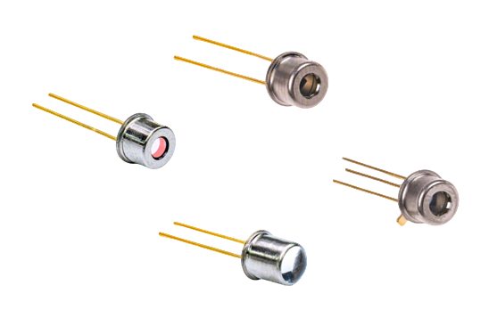
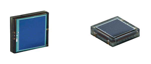
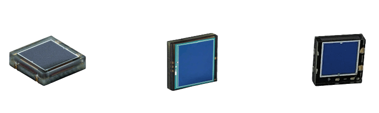
Core components in the field of medium and high-precision optical signal detection

Extremely low dark current (Max 5pA), minimal noise interference, capable of accurately converting weak light signals and improving detection precision;
The flat window has uniform light transmittance, suitable for scenarios with high requirements for light signal uniformity, and no additional optical correction is needed

The spherical window/optical window has light-gathering properties, which can enhance the intensity of local optical signals and is suitable for signal collection in low-light environments;
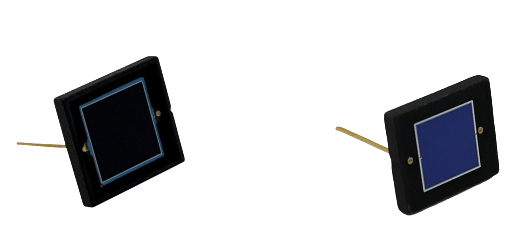
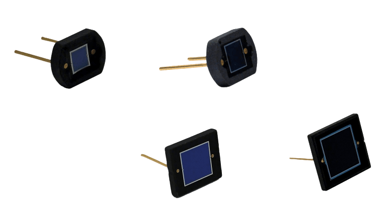
The 2pin pin design simplifies circuit connections, reduces the difficulty of device integration, and at the same time, the dark current (Typ 2pA) is extremely low, resulting in a high signal-to-noise ratio.

The 3pin pin design supports more complex circuit function expansion (such as additional signal calibration and temperature compensation pins), making it suitable for multi-functional optical detection equipment;
The flat window ensures the uniformity of optical signals. Combined with the 1.1×1.1mm photosensitive surface, it balances signal intensity and uniformity in medium light intensity scenarios.
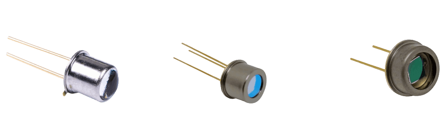
Large photosensitive area (Φ1.5mm) increases light input, adapts to signal acquisition in low-light environments, and enhances signal strength without relying on light-gathering components;
2pin pins simplify integration, the flat window ensures uniformity of optical signals, and the dark current (Max 20pA) remains at a low level in the large photosensitive area model, balancing light input and signal accuracy

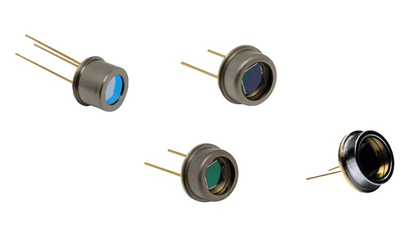
Large photosensitive area (Φ1.5mm) + spherical window combination, double enhancement of weak light signal intensity: the large photosensitive area increases light intake, and the spherical window condenses light to enhance local light density, adapting to extremely weak light environments;
Inheriting the stability of the TO18 package, signal acquisition can be achieved without complex optical systems in extremely weak light scenarios, reducing the overall cost of the equipment.
Core devices in the fields of low-light detection and precision measurement

Miniaturized design, which can be embedded in space-constrained devices such as portable spectrometers, with a volume more than 80% smaller than the largest model; low dark current + low junction capacitance, with the highest precision in weak light detection (capable of capturing nW-level optical signals), and high-frequency response without delay.
Compatible with 260℃<5s lead-free reflow soldering, suitable for mass production of micro devices.

It has higher absorption efficiency, is suitable for medium-intensity optical signal detection, and balances dark current and rise time, ensuring both detection accuracy and meeting the response speed requirements of most scenarios.
Compatible with lead-free reflow soldering, it can be batch-integrated into industrial-grade optical equipment (such as liquid chromatography detectors).

The circular photosensitive surface is compatible with circular optical path systems (such as laser collimators and circular probes), and its optical path coupling efficiency is 15% to 20% higher than that of the square one. It can directly replace the square model to adapt to circular optical designs without adjusting the circuit.
It works stably over a wide temperature range, making it suitable for outdoor light detection scenarios or non-standard optical paths.

The photosensitive area reaches 13.69mm², with stronger low-light capturing capability (especially suitable for large-area uniform light field detection); it has high shunt resistance and low leakage current, and the long-term monitoring signal stability is better than that of small-size models.
It is compatible with industrial-grade equipment installation and can be directly integrated into standard optical instrument slots.

The photosensitive area reaches 33.64mm², making it suitable for detecting extremely low light intensity and large-area optical signals (such as ambient dim light monitoring).
It has a wide operating temperature range (-20~+80℃), with small dark current drift in high-temperature environments, making it suitable for complex environments like industrial workshops; it is compatible with lead-free reflow soldering and can be batch-integrated into large optical analysis equipment.
Light-sensitive area: 100mm² (the largest among 6 models), with high light absorption efficiency, capable of capturing extremely weak and large-area scattered light signals such as faint starlight in the starry sky and long-distance optical communication signals; the large size is compatible with large probes, enabling the reception of wide-range light signals without optical focusing.
Industrial-grade ESD protection (1000V HBM), ensuring stable operation in strong electromagnetic interference environments (such as next to factory frequency converters).
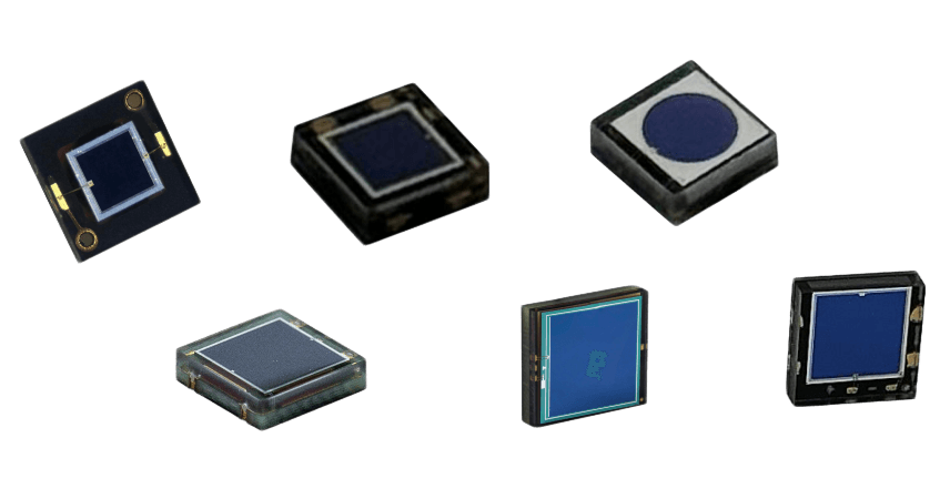
High-precision photodetection device based on silicon-based PIN structure
High-precision low-light detection: low dark current + low junction capacitance, capable of capturing weak light signals at the nW level.
Miniaturization + fast response: the smallest photosensitive surface, can be embedded in small devices such as portable instruments, with a rise time of 0.15μs, suitable for high-frequency optical signal monitoring such as short-distance optical communication feedback.

It has higher light absorption efficiency, with a dark current only 0.4 times higher, balancing detection accuracy and light capture capability; it is compatible with PCB board slots of most industrial equipment, no need for custom interfaces, and can be integrated in batches.
It features a full spectral response from 350 to 1060nm, suitable for visible light detection (such as LED power) and near-infrared monitoring (such as 800nm ambient light).

Optimized for a peak wavelength of 800nm, the near-infrared band (760~1060nm) is suitable for detection scenarios dominated by near-infrared; the peak optimization compensates for the weak near-infrared response of ordinary models.
It can directly replace the latter to adapt to near-infrared equipment without adjusting the circuit or optical structure.

Light-sensitive area: 33.64mm², with high light absorption efficiency, capable of capturing extremely weak large-area scattered light at the μW level; large-size products still use through-hole packaging, making later maintenance, insertion, removal and replacement convenient without the need to desolder the entire board.
Wide operating temperature range (-20~+80℃), low dark current drift coefficient at high temperatures, suitable for complex environments such as industrial workshops and outdoors.

The photosensitive area reaches 100mm², and it can receive a wide range of optical signals without optical focusing. It can capture extremely weak and scattered light signals such as faint starlight and long-distance optical communication signals.
The structure is sturdy, and with wide temperature range and anti-interference design, it is suitable for long-term continuous operation (such as 24-hour ambient light monitoring).
Silicon PIN structure photoelectric conversion device

The miniaturized design can be embedded in portable devices (such as handheld instruments).
Low dark current + fast response can accurately capture nW-level weak light and high-frequency light signals, and the wide temperature range is suitable for outdoor/industrial temperature difference environments.

The large spherical lens can concentrate light, with a low-light capture efficiency of over 20%. It can improve detection sensitivity without additional optical components.
Applications: Low-light ambient light monitoring, low-power laser signal reception, and auxiliary for medical low-light imaging.

A balance between size and performance, with a photosensitive area twice as large as that of the PDCT01 series, resulting in higher light absorption efficiency.
At the same time, it retains the characteristic of low dark current, making it suitable for most general detection scenarios.

Light-sensitive area: 35%. The signal is more stable during medium and high light intensity detection. Shunt resistance: Min. 3GΩ (excellent insulation, small leakage current).
Applications: Industrial optical power monitors, packaging film light transmittance detection, medium-precision luminous flux testing.
The photosensitive area is slightly larger, resulting in better uniformity when detecting large-area light fields (such as display backlights). It is compatible with the circuit design of PDCT14-001 and can be directly replaced for upgrading.
Applications: Detection of display backlight uniformity, light intensity monitoring of large-area LED modules, multi-channel optical signal collection.

The ultra-large photosensitive area can capture extremely weak, large-area scattered light (such as μW-level optical power). The TO8 packaging structure is sturdy, with strong resistance to impact and electromagnetic interference.
It is applied in night security light monitoring, Fourier transform infrared spectrometers, and overall light intensity detection in greenhouses.
Silicon-based PIN structure photoelectric conversion devices optimized for response efficiency in the near-infrared band

It has better low-light detection accuracy, suitable for detecting extremely weak light signals at the μW level; it has a faster high-frequency response speed, capable of capturing pulsed near-infrared signals below 1MHz (such as infrared remote control coding, short-distance infrared communication feedback).
It has strong versatility in the medium and short near-infrared range, and can be adapted to multiple near-infrared detection scenarios without replacing components.
It has outstanding large-area detection capability and is suitable for scenarios requiring large-scale optical signal collection, such as "greenhouse environmental light intensity monitoring and large optical analysis equipment"; the long near-infrared range has strong pertinence and is a dedicated choice for industrial 1064nm laser power monitoring and long-distance infrared sensing.
It has higher environmental durability and can operate stably in industrial environments with high humidity (10%~90% RH) or slight dust without additional protection.
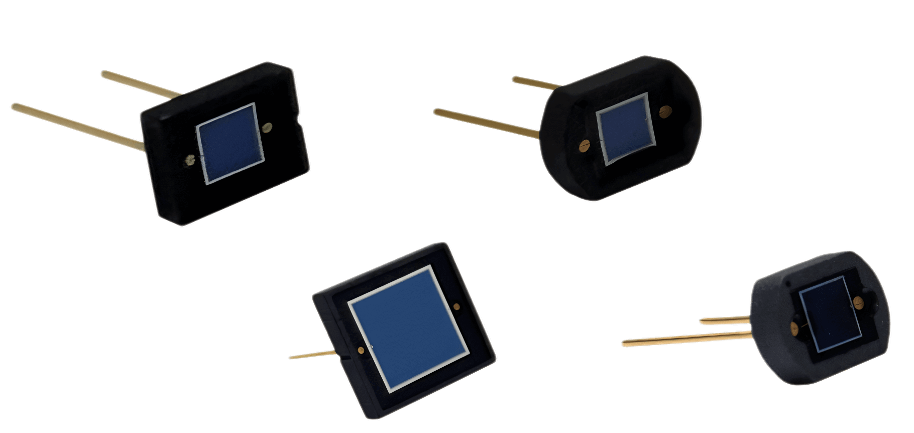
A passive photoelectric conversion functional device with a dual in-line package (DIP) through-hole package.
High-speed response: With a rise time of 50μs and a low junction capacitance of 300pF, it captures high-frequency near-infrared signals faster, reduces signal delay, and is suitable for high-speed optical signal detection scenarios.
Low noise: A maximum dark current of 0.9pA and a low equivalent noise power can further reduce detection noise, ensuring the accuracy of weak near-infrared light signal conversion.

High photosensitive area and adaptation to specific wavelengths: A larger photosensitive surface can receive more near-infrared light, making it suitable for scenarios requiring high light flux or detection of specific long-wavelength near-infrared rays.
High potential for photocurrent output: A larger photosensitive area combined with a light response adapted to 1064nm can output a larger photocurrent under the same light intensity, reducing the design difficulty of subsequent signal amplification circuits.
Silicon-based PIN junction near-infrared optimized photoelectric conversion device.

A rise time of 0.04μs is the fastest in the series, enabling precise capture of high-frequency pulsed near-infrared light signals with no signal delay.
It offers the best weak light detection accuracy, making it suitable for precision scenarios sensitive to noise; it can be embedded in space-constrained devices (such as miniature optical power meters).

The large spherical lens window can converge divergent near-infrared light, increasing the luminous flux by 30% to 50% (compared with flat windows), and is suitable for low-light environments (such as low-power laser detection, optical analysis in dim scenes).
The lens is integrated into the package, eliminating the need for an external condenser lens, simplifying circuit design, and reducing device size and cost.

One additional pin can serve as a "shield terminal" (grounded to isolate electromagnetic interference) or a "strobe terminal" (an external voltage to control the switching of devices), making it suitable for complex industrial electromagnetic scenarios (such as motors, equipment around frequency converters).
If the pin is configured as a shield terminal, it can reduce the interference of external electromagnetic radiation on the photocurrent and ensure the signal stability of optical analysis equipment.
The large photosensitive surface can receive more near-infrared light, making it suitable for high-light-intensity scenarios (such as high-power laser power monitoring).
It has stronger resistance to mechanical impact and temperature changes, and is suitable for harsh industrial environments (such as equipment monitoring in high-temperature and vibrating conditions).
A broad-spectrum photoelectric conversion device whose spectral response covers the ultraviolet to near-infrared bands.

The photosensitive surface size is 1.0×1.0mm, suitable for space-constrained scenarios; it has strong stability in converting high-frequency optical signals and can withstand a wide temperature range environment.
It is suitable for high-frequency optical power detection, such as monitoring of 1000nm near-infrared pulsed optical signals and cross-band optical sensing in miniaturized optical devices.
Compatible with mainstream industrial welding processes, with strong adaptability for mass production; stable detection in low-light environments (such as low-intensity ultraviolet 365nm light); anti-static interference capability meets the needs of industrial scenarios.
Suitable for optical analysis equipment, such as multi-band spectrometers (requiring simultaneous detection of ultraviolet 200nm, visible light 633nm, and near-infrared 1000nm light), and light intensity monitoring in industrial production lines (relying on anti-static and welding adaptability).

It has better linearity of photocurrent, can withstand extreme storage environments, and has strong adaptability to transportation and inventory. The transmittance of quartz optical window to ultraviolet light is 30% higher than that of ordinary glass, improving the accuracy of ultraviolet detection.
It is suitable for ambient light monitoring equipment, such as outdoor ultraviolet radiation intensity detection (relying on quartz optical window and wide temperature working range), and weak light near-infrared signal capture (relying on large photosensitive surface and high shunt resistance).

Operating temperature: -20~+80℃, suitable for consumer electronics and general industrial environments. The welding time is shorter than that of the TO series (10s), improving mass production efficiency; the number of pins is 2, the circuit connection is simple, no complex peripheral adaptation is required, and the research and development cycle is short.
It is applicable to the field of consumer electronics, such as ambient light sensors in mobile phones and tablets (relying on DIP packaging and low cost), and miniaturized optical power meters (relying on low dark current and medium and low frequency stability).

It has better low-light detection accuracy; it is compatible with DIP standard slots, making replacement convenient during later equipment maintenance and reducing maintenance costs; the maximum reverse voltage is 20V, which is 50% higher than some similar models, improving the voltage resistance of the circuit.
It is suitable for small and medium-sized optical analysis equipment, such as laboratory ultraviolet-near-infrared spectrophotometers (relying on wide-spectrum response and convenient maintenance), and light intensity consistency detection in industrial quality inspection (relying on large photosensitive surface and voltage resistance).

Highest sensitivity in low-light response; welding temperature of 260℃/5s, with strong compatibility for mass production; maximum reverse voltage of 20V, eliminating the need for additional voltage-reducing components in circuit design and simplifying peripheral circuits.
Suitable for devices with high requirements on photosensitive area, such as pulse oximeters in the medical field (relying on high sensitivity to near-infrared 1000nm) and wide-spectrum light intensity collection in large environmentaPackage Typel light monitoring stations (relying on large photosensitive area and extreme storage stability).
Optoelectronic conversion device with enhanced ultraviolet band response and COB package integration.
The module has the optimal response speed to high-frequency optical signals, minimal dark current interference in low-light environments, and higher detection accuracy; it also features better photocurrent linearity, reducing signal distortion.
Small-sized photosensitive surface + low junction capacitance, suitable for compact space detection.

Resin windows have strong cost adaptability, balancing detection accuracy and economy, making them suitable for batch and general-purpose scenarios; they have a stable noise suppression effect on medium-intensity light signals.
They are applicable to general-purpose optical detection equipment, such as regular ultraviolet light intensity monitoring in industrial production lines and basic light signal collection in small and medium-sized optical analysis equipment.

The medium-sized photosensitive surface improves light absorption efficiency, is suitable for detecting medium-intensity light signals, has a stronger ability to capture light signals, and reduces signal missed detection.
The junction capacitance and rise time are adapted to medium and low-speed light detection scenarios, without the need for complex peripheral circuit optimization, and the R&D adaptation cost is low.

Designed with the largest photosensitive surface, it has the optimal capability to capture large-area and strong light signals. It can cover a large detection area without the need for multiple chip arrays, reducing integration complexity.
Although it has relatively large dark current and junction capacitance, it is suitable for low-frequency strong light detection scenarios. It does not require high-frequency response optimization and is suitable for scenarios where the detection area requirement is higher than the response speed requirement.
Optoelectronic conversion devices with DIP dual in-line package

The small-sized photosensitive surface is suitable for compact circuit design, and the low dark current reduces noise interference in low-light detection.
The fast rise time can capture fluctuations in high-frequency optical signals, and its comprehensive performance is suitable for high-precision low-light detection scenarios.
Enhance the response speed in the ultraviolet band. In the detection of weak ultraviolet light (such as low-power UV LEDs), the signal capture efficiency is better than that of non-optimized models of the same size.
It is suitable for conventional ultraviolet light intensity monitoring in industrial production lines (such as light intensity calibration of UV curing equipment) and conforms to the application scenario of "light power detection".

Small size + quartz window design, meeting both the needs of compact layout and deep ultraviolet detection.
It avoids the space occupation problem of large-size quartz window models and is suitable for small deep ultraviolet sensing devices.

The medium photosensitive surface balances light absorption efficiency and circuit space. The clear peak wavelength facilitates the matching of optical systems, making it suitable for scenarios with high requirements on wavelength response consistency.
It is applicable to the optical signal receiving module of small and medium-sized optical analysis equipment (such as ultraviolet spectrophotometers), matching the application direction of the document "Optical Analysis Equipment".

A large photosensitive surface improves the capture efficiency of medium-intensity light signals, enabling coverage of a relatively large detection area without the need for a multi-chip array.
It reduces the complexity of circuit integration and is suitable for medium-power light detection scenarios.

The combination of a medium-sized photosensitive surface and a quartz window not only meets the requirements of deep ultraviolet detection but also avoids the high cost of large-sized quartz windows, making it suitable for medium-power deep ultraviolet light monitoring scenarios.
It is applicable to light intensity monitoring of industrial-grade deep ultraviolet curing equipment and medium-sized water quality ultraviolet sterilization detection systems, expanding "light power detection" to the medium-power deep ultraviolet field.

Designed with the largest photosensitive surface, it can cover an ultra-large detection area without the need for multi-chip splicing. It is suitable for detecting strong light and large-area optical signals, and reduces the complexity of the optical system inside the device.
It is suitable for optical power density monitoring of large-scale ultraviolet curing equipment (such as curing of wide-format plastic parts) and industrial-grade large-area strong light detection terminals, matching high-power scenarios of "optical power detection".

The largest photosensitive surface is combined with a quartz window, which takes into account both large-area detection and deep ultraviolet response. It is suitable for special scenarios that need to meet both "large detection range" and "deep ultraviolet monitoring" simultaneously, without the need for multiple device combinations.
It is suitable for light intensity monitoring of large-scale deep ultraviolet disinfection equipment (such as ultraviolet disinfection channels in sewage plants) and light power detection of wide-format deep ultraviolet curing production lines, expanding "light power detection" to the ultra-large range deep ultraviolet field.
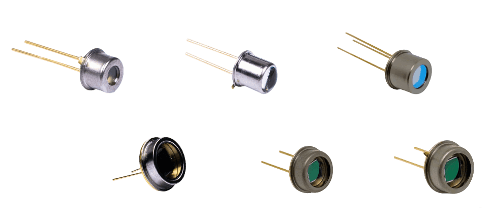
Optoelectronic conversion device with TO transistor package and metal hermetic sealing
The small-sized photosensitive surface is suitable for compact circuit designs. The low dark current (30pA) reduces noise interference in weak light detection, and the fast rise time (0.13μs) can capture fluctuations in high-frequency optical signals.
The optical glass window has strong cost adaptability and is suitable for mass general scenarios.

The combination of small size and deep ultraviolet detection capability avoids the space occupation problem of large-sized quartz window models; the quartz window is resistant to ultraviolet aging, and the light transmittance attenuation after continuous ultraviolet irradiation is lower than that of optical glass, extending the service life of the device.
It is suitable for handheld ultraviolet sterilization effect detectors (for detecting 254nm sterilizing ultraviolet light) and small water quality ultraviolet disinfection monitoring modules, expanding "light power detection" to the deep ultraviolet field.

The medium-sized photosensitive surface balances light absorption efficiency and circuit space, making it suitable for small and medium-sized detection equipment.
Suitable for conventional ultraviolet light intensity monitoring in industrial production lines and small and medium-sized optical power meters.

The combination of a medium photosensitive surface and a quartz window is suitable for medium-power deep ultraviolet detection.
It is applicable to the light intensity monitoring of medium-power deep ultraviolet curing equipment and medium-sized water quality ultraviolet sterilization effect detectors, expanding "light power detection" to the field of medium-power deep ultraviolet.

It can meet the needs of large-area light detection without switching to the TO8 package, balancing cost and detection efficiency.
It is suitable for light signal receiving modules of laboratory-grade optical analysis equipment (such as ultraviolet spectrophotometers) and small and medium-sized large-area optical power calibration equipment.

The only model that achieves "deep ultraviolet detection + large light absorption area" under the TO5 package. It does not require the use of a larger TO8 package and is suitable for deep ultraviolet optical analysis scenarios sensitive to size.
Suitable for small deep-ultraviolet spectrophotometers and portable deep-ultraviolet optical power analyzers, expanding "optical analysis equipment" to the deep-ultraviolet field.

The TO8 packaging structure is more robust (suitable for harsh industrial environments) and can cover an ultra-large detection area without the need for multi-chip splicing, reducing integration complexity.
It is suitable for optical power density monitoring in large-scale ultraviolet curing equipment (such as wide plastic parts and PCB board curing), and industrial-grade large-area strong light detection terminals.

It features TO8 packaging for industrial environment resistance, supports deep ultraviolet detection, and has an ultra-large photosensitive surface to meet the needs of capturing large-area strong light, eliminating the need for combining multiple devices to cover complex scenarios.
It is suitable for light intensity monitoring of industrial-grade deep ultraviolet disinfection equipment (such as ultraviolet disinfection channels in sewage plants) and light power detection in wide-format deep ultraviolet curing production lines, expanding "light power detection" to the industrial-grade deep ultraviolet field.

